Update: This has been confirmed to work on a Barco ADVM 28 also
Note: This was originally only targeted the ADVM14. As time went by I’ve modded all but the ADVM28, and added info here, which may make it seem a bit confusing read. Sorry 🙂
The Barco/BarcoNet/Scientific Atlanta ADVM line (ADVM10/14/20/28) is notorious for its weird selection of inputs. Two composite, S-Video and SDI, but no component/RGB, makes it somewhat unfavorable for many CRT enthusiasts, so RGB modding it has been on the list for many. Many of the previous mods, at least the ones I know of, revolved around hijacking the SDI input and using a RGB->YUV converter. This seems to work with various success, depending on the version of the monitor seemingly, again I am not an expert on this brand or unit, but since the unit has no less than 2 jungle ICs, and one has two unused RGB inputs, I thought that was the way to attack it instead. I am unsure of how much the various versions of this monitor differ, mine is BarcoNet branded.
Update: So it seems there are multiple “generations” of the Barco ADVM monitors. The early (around 2000) units (at least of ADVM20/28) “only” have a single composite channel, S-Video and SDI with no passthrough. I have modded one of these using the same method, and it works fine. To avoid losing composite/S-Video, I chose to use blanking from SCART instead of from the Arduino.
Now the “secondary” jungle is the one dealing with S-Video and composite, a Philips TDA9321H. This unit has two unused RGB inputs, RGB1 and RGB2, where RGB1 can be converted to YUV at the same time, so some form of YPbPr should also be possible. That road is yet unexplored. I chose to start out with RGB2 to risk the fewest issues to begin with.

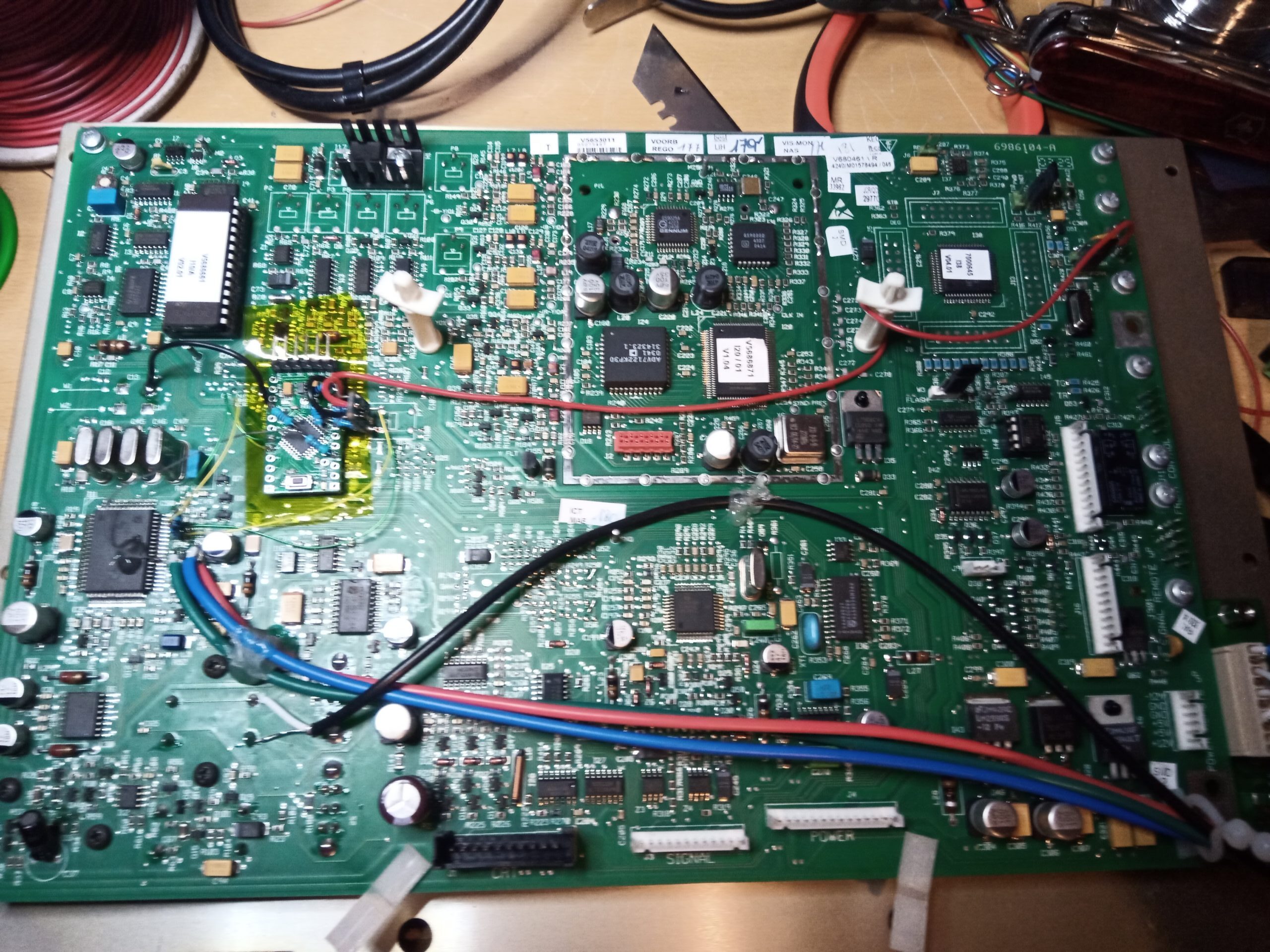
The signal board that needs to be worked on is on the back plate of the monitor, so unscrew a million screws and get that board out. When done, you should have this:

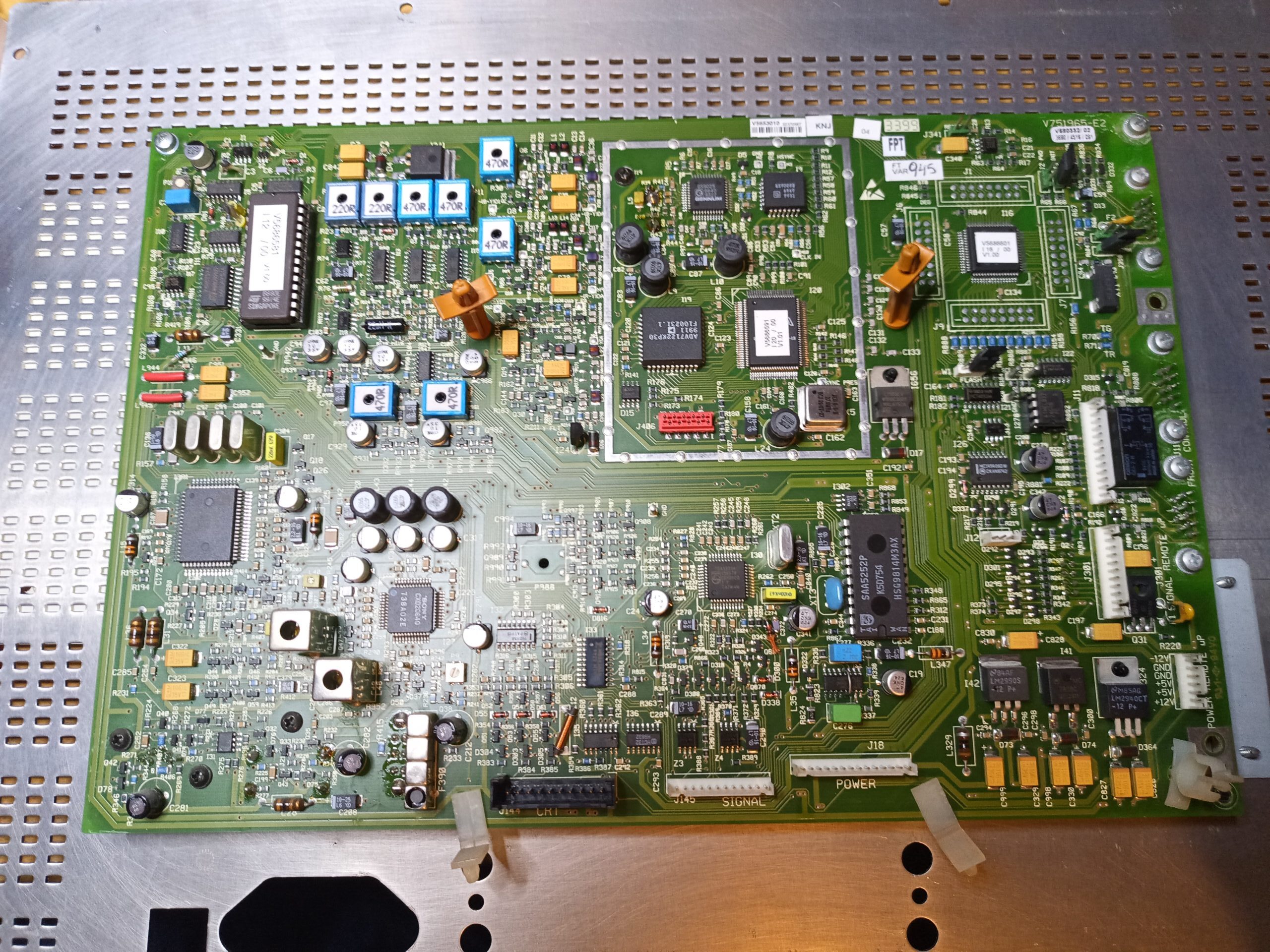
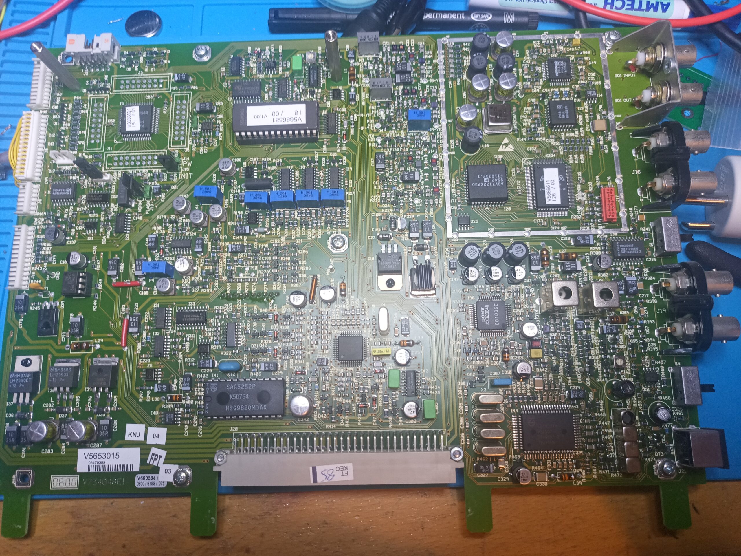
Now the TDA9321 is the one in the middle left (I put a sticker on here with some lines showing the pins) its reference is I11.


Now firstly, I verified with a logic analyzer that the RGB inputs really were disabled in software, and sure enough, the tenth register, 0x0A is constantly written as 0x00. Here are the values that are constantly sent to the monitor, first is the hex address, next is the hex value, last is the value in binary:
00 - CF - 1100 1111
01 - 20 - 0010 0000
02 - 00 - 0000 0000
03 - 20 - 0010 0000
04 - 00 - 0000 0000
05 - 84 - 1000 0100
06 - 04 - 0000 0100
07 - 00 - 0000 0000
08 - 02 - 0000 0010
09 - 22 - 0010 0010
0A - 00 - 0000 0000 YUV/D3=0 ECL/D2=0 IE2/D1=0 IE1/D0=0
0B - 01 - 0000 0001
0C - 41 - 0100 0001
0D - 1F - 0001 1111
0E - 3F - 0011 1111
If we check the datasheet, this means the following:

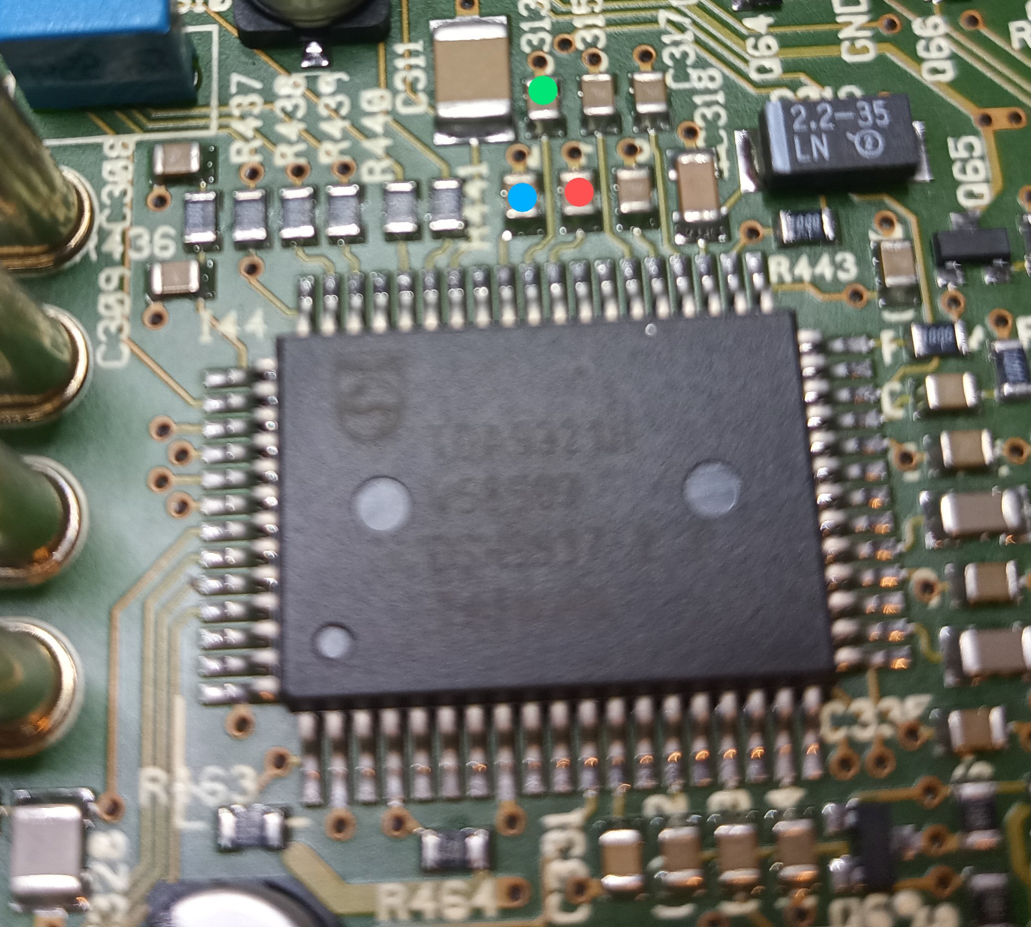
At the same time, RGB1 (and RGB2) are both directly connected to GND (no pulldown resistor) which means no matter what, we need to lift pin(s) which always suck due to the risk of breaking them.
Another interesting observation is that it does not change the input/output registers (0x08 and 0x09) depending on CODED A or CODED B is selected, which I guess means that the signal is switched elsewhere. It would have been nice to be able to distinguish which signal was selected, but only SDI and S-Video selections trigger actual changes to these values.
Update: So the composite video is switched via a TDA8540 video mux IC (I21), more or less the largest IC to the right in picture 2 above. When CODED1 is chosen, register 0x00 (SWI) is written to 0x80 and when CODED2 is chosen, register 0x00 is written to 0xC0, so OUT3 switches between INPUT1 for CODED1 and INPUT0 for CODED2, and OUT3 is then apparently connected to the jungle (through at least a comb filter IC also, a TDA9181). This does not apply to the early generation ADVMs as they don’t have the TDA8540 and the TDA9181, but instead “just” a Sony CXD2064Q comb filter.
Anyways, first of all we need to renable IE1 and/or IE2. Just as with the JVC monitors that did something like this, the “obvious” choice is to intercept I2C communication and change the data sent to register 0x0A from 0x00 to at least 0x03, as that would set the two lowest bits to 1, thus enabling IE1 and IE2 as per table 27 and 28 of the datasheet:

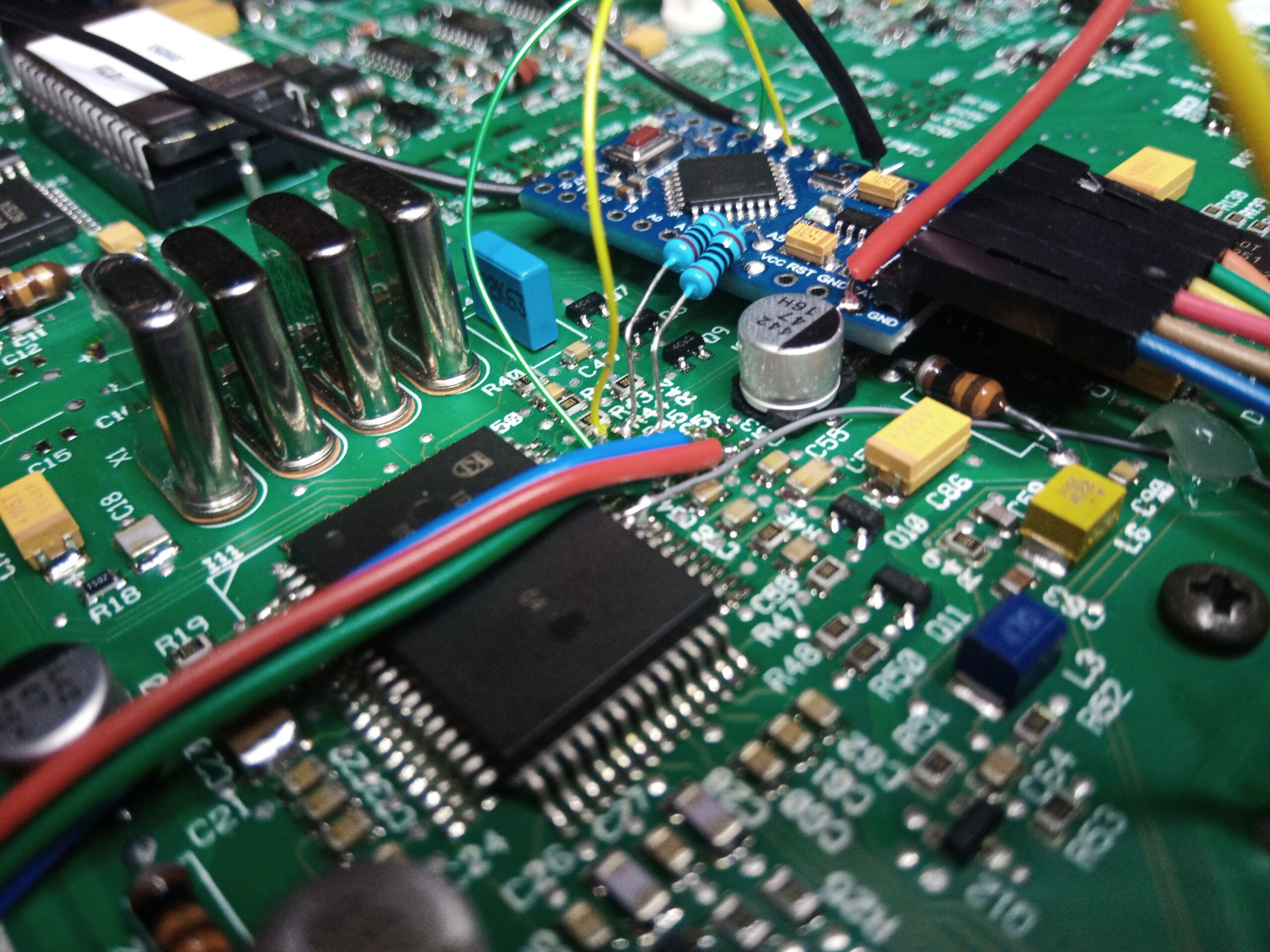
So just as with the JVCs the jungle needs to be isolated from the I2C network of the monitor. This is done by removing R44 (SDA) and R45 (SCL) resistors which can be seen just above the chip to the left from the previous picture 3. These two are the 100R “termination” resistors or whatever we call them, added to minimize signal reflection and such. I then wrote a small Arduino sketch that makes the MCU act as a middle man, and forward the data from the monitor to the jungle, and back, but changing the 0x0A data to 0x03. You can find the sketch here.
Now I used a Mini Pro board, where the hardware I2C is connected to pins A4 (SDA) and A5 (SCL). Connecting these two pads through a new 100R resistors, connected to the pads farthest away from the chip, will make the Arduino act as the TDA9321H. Now to relay the information back to the original jungle, the sketch creates a “software” I2C master line on D4 (SDA) and D5 (SCL) and we thus need to connect those to the two closest pads of R44 and R45, so it can speak to the jungle. Remember to add pull-up resistors to those two lines, so a 2.2-3.3k from D4 and D5 to the Arduinos 5V pad.
On the “early” generation, the resistors are R200 (SDA) and R201 (SCL).
On ADVM10 they’re R440 (SDA) and R441 (SCL).
Power to the MCU can be taken from the large 7808CV regulator in the top of the board, and feed it to the RAW input of the Mini Pro (or similar if you’re using a Nano 3.0 etc). Same goes for GND, but there are also plenty of large GND pads scattered around the board.
If the Arduino is programmed correctly, you should be able to start the monitor up, connect a composite video signal, and apply 1-3V to RGB2 to see the screen go black (because nothing is input to RGB input pins yet).
Now how the Arduino program works apparently influences a lot how everything goes. I spent some time tweaking it until it now seemingly works, otherwise the screen would start to flicker, tear and seemingly go out of sync. I think this is because of the two I2C lines from time to time influencing the timing in regards to each other, as the MCU is single core, but the current revision seems to fare fine. I am contemplating switching to a RP2040 or similar, but that would then require level translations as the jungle needs at least 3.5V for a high signal, and the RP2040 is a 3.3V system. For now I’d like some feedback as to how the current Arduino method works.
The three color signal inputs are BI2, GI2 and RI2, which are “grounded” through C51 (BI2), C52 (GI2) and C53 (RI2) which are just right of the R44 and R45 resistors. On the early generation these are C177 (BI2), C173 (GI2) and C178 (RI2). These need to be removed, and the corresponding pads closest to the jungle, are where the RGB signals should be connected, through a 0.1uF capacitor, and a 75R termination resistor to GND, like this:
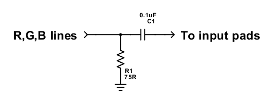
The lifted RGB2 pin, should be connected to a blanking signal between 1-3V. If SCART pin 16 is used, a 75R resistor to GND is advised, otherwise take appropriate measures to create a compatible voltage, eg. through voltage dividing the 8V, so something like a 22K and a 8.2K will give roughly ~2V. Sync should be fed directly to one of the CODED A/B inputs, I suggest CODED A, if you’re using BNC you can just plug it in, if you’re using SCART, solder sync wire to the center pin of the BNC plug on the PCB.
When everything is hooked up, mine looked like this:
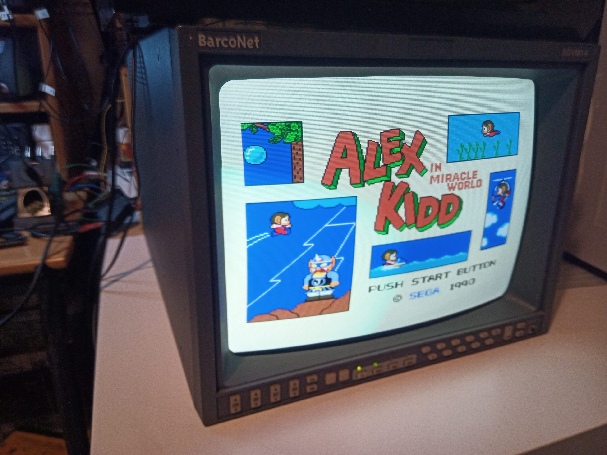
After doing this, you should now be able to input a RGB signal while blanking with 1-3V on RGB2 pin. Here’s the monitor with SEGA Master System 1 connected. The picture’s bottom part blurriness is my phone, not the image of the screen 🙂
So that’s it! Let me know if you try this, and what issues you run into…
Wiring up RGB
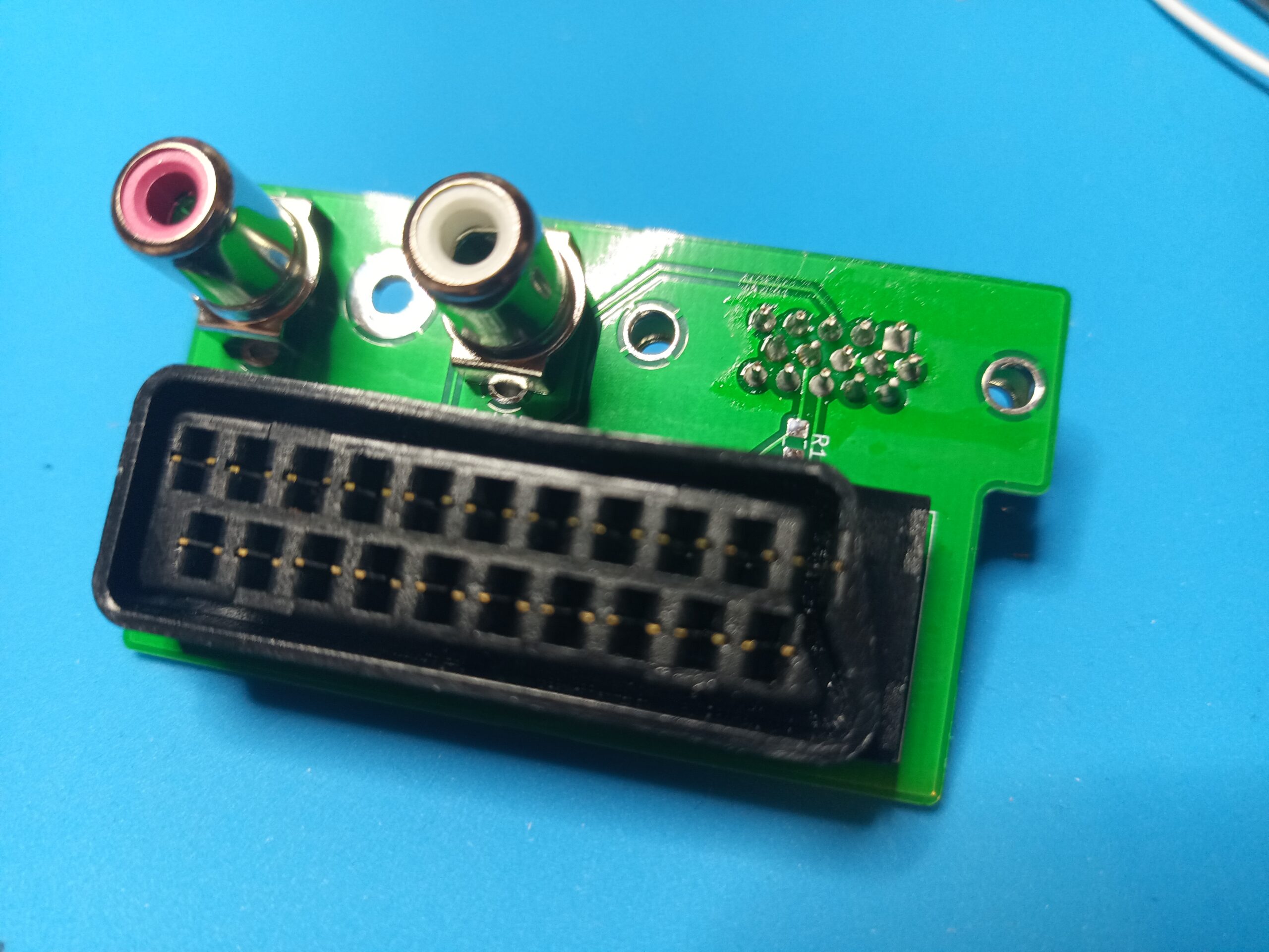
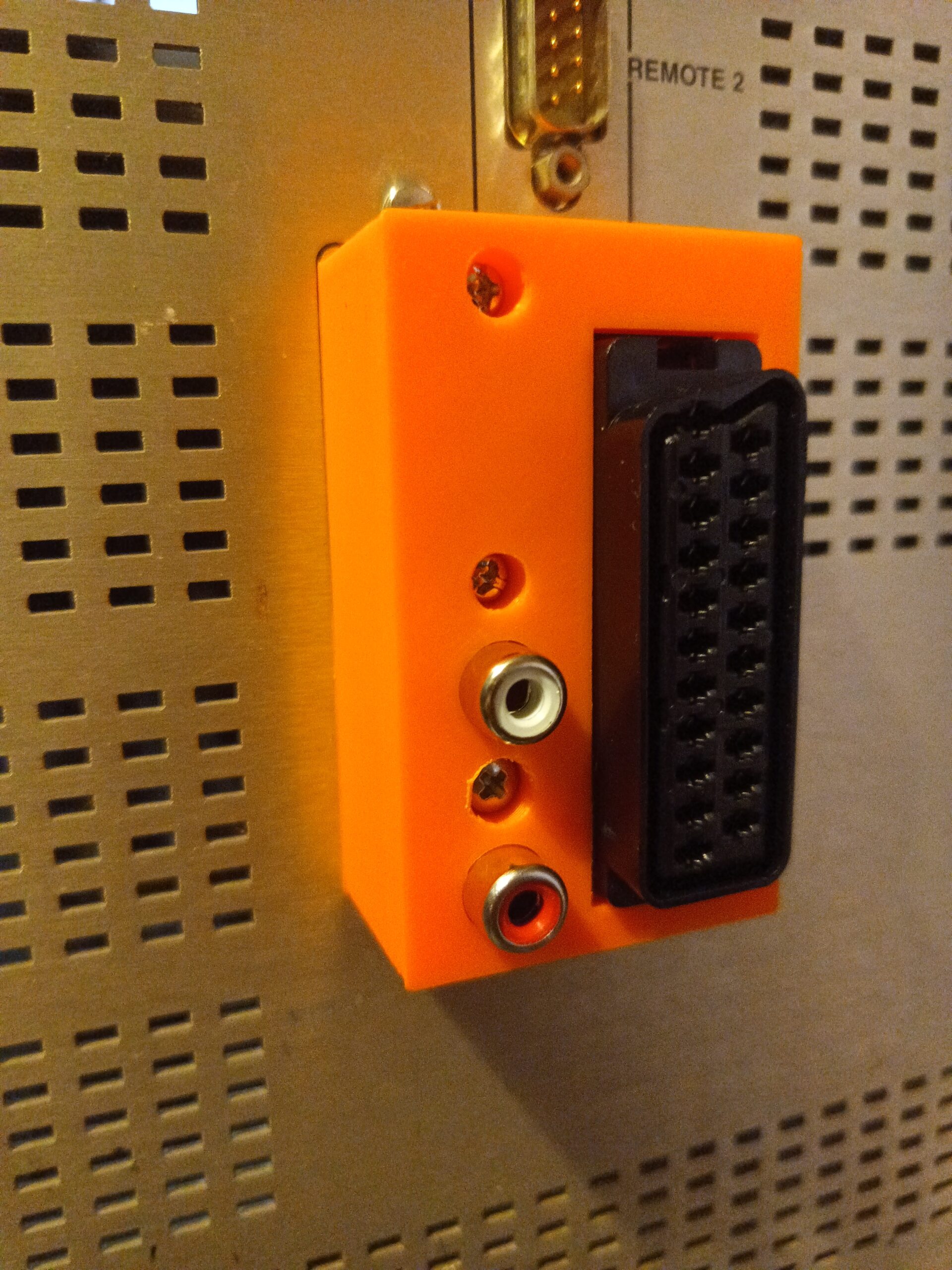
So Barco chose this fancy backplate all in metal, which I didn’t want to ruin. There is however an unused DE-9 cutout labelled “RS485”, which I thought would be nice to install a HD15/VGA port in, to avoid any drilling, especially because VGA breakout cables exist in many forms. I thus created a small PCB that can accomodate a HD15 port and the termination resistors plus DC bias caps, kinda like my previous SCART breakout board, and paired with a couple of 7mm M3 standoffs, fit perfectly in the space.


You can find the KiCad project here: https://github.com/skumlos/HD15-RGBS-Input
I then wired some shielded 75R mini-coax cables from the board to the input pads, so it looked like this:

The mini-coax is a Tasker C263 cable I split up.
ADVM10 notes: Don’t run the cables over the signal board, but around the *back* of the board, like here. If you run it over, you most likely won’t be able to put the top cover on.
For the early generation ADVM, I chose to use blanking from SCART. The HD15 board supports adding a 75R resistor (R21) for HD15 pin and then use this pin as blanking. Then “short” the bottom pads of the footprint for the manual switch like so:

The BLANK(ing) pin from the connector is then wired to RGBI2 pin on the jungle.
Since pin 9 is rarely broken out in HD15/VGA breakout cables, I chose to make a small SCART to HD15 board that runs blanking to pin 9.

Find the Kicad project for the SCART-to-HD15 board here: https://github.com/skumlos/scart-to-hd15
Download the 3D printable shell here: https://www.thingiverse.com/thing:6484206
Auto blanking to RGB (only applies to “new” ADVMs)
You might’ve noticed the above picture now has two Arduino Mini Pro’s. This is because the HD15 setup has a “problem” and that is blanking. VGA breakout cables usually just go to 5 BNCs or something, so there is no apparent means of blanking. The 5V/KEY pin of VGA plug, would be obvious, but again, usually not broken out. Also, I still didn’t want to drill the backplate and install a switch.
So my plan was to make the monitor automatically blank, when CODED1 was selected. By that I would still have CODED2 for composite and S-Video. Problem is I thus needed a way to know which composite input is selected. There are a bunch of options that makes sense:
The TDA9321H has multiple composite inputs, so I actually thought I could simply check which one here, but switching between CODED1 and 2 doesn’t trigger anything.
Then there’s a TDA9181 comb filter has two inputs, so I thought the two composite video inputs were switched there, but no.
I found out it’s switched in a TDA8540 video mux (I21) as written/appended earlier. This mux has a couple of outputs that *could* have been used to further switch other signals, like audio, but those weren’t used either, so only one thing to do: Intercept the I2C signal to the TDA8540. Problem was then, that when I attached two Arduinos to the I2C line of the monitor, it stopped working. This must be because of the push/pull abilities of the I2C master, and the requirements of the Arduinos I/O pins (at least that’s my best explanation), so I had to turn it into a “sniffer” instead (which is fine, as we don’t actually need to change any data, only listen). So to do this, the second Arduino’s I2C lines A4/SDA and A5/SCL was “prefixed” with a non-inverting buffer and a 100 Ohm resistor like so:
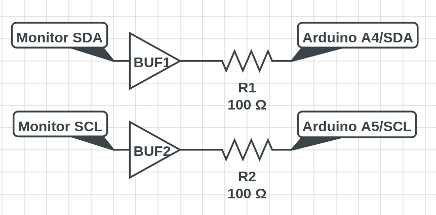
I used a SN74LVC2G34DBV on a small SOT-23 breakout, and then supply it from the Arduino Mini Pro’s 5V and GND outputs. The 100R is to ensure that when the I2C line is released by master (and thus pulled-up) then the Arduino’s ACK part of the I2C communication protocol (where it pulls the SDA line low) won’t “short out”. Thus a 1K or similar might be just as good. The Arduino then pulls its D13 line HIGH when CODED2 is chosen, and LOW when CODED1 is used. This signal is then passed onto the other Arduino which then based on the video switch signal blanks if composite is selected *and* CODED1 is selected. Blanking pin is D13 in the TDA9321H, and the 5V output of the pin is run through a voltage divider consisting of 2x1K resistors, so the resulting 2.5V is used as the actual blanking signal.
I put the Arduino sketch for the TDA8540 sniffer here: https://github.com/skumlos/tda8540-sniffer
Update: Doing it with a single MCU
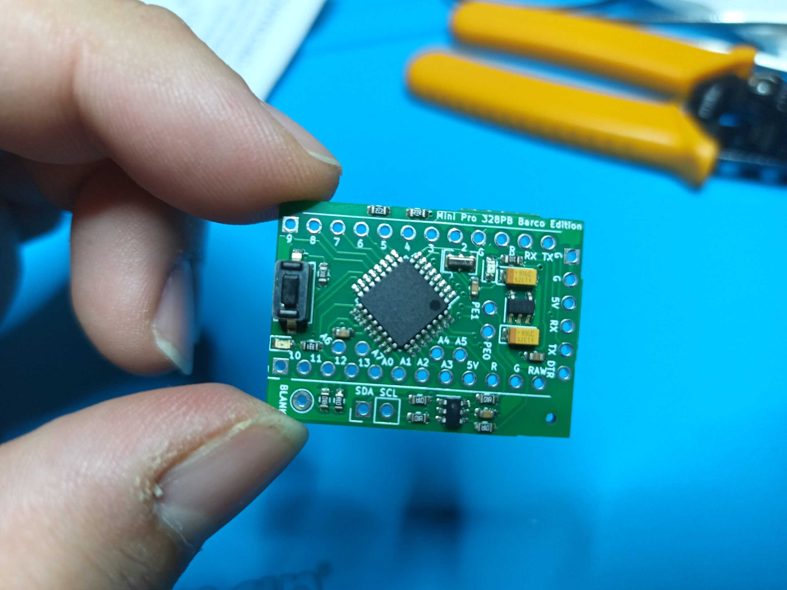
I really don’t dig the two Arduinos, so I made a “clone” of it which uses the ATMEGA328PB as it has two I2C ports. PE0 is SDA1 and PE1 is SCL1. Note that to use it, you need support fore Wire1, which can be found in MiniCore board support in Arduino IDE.
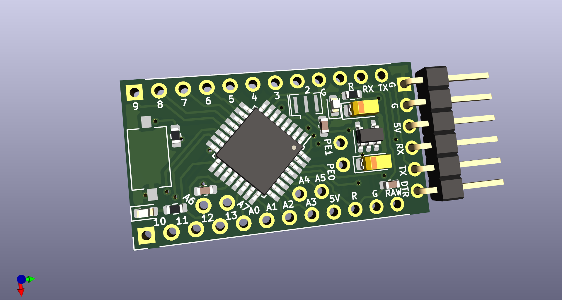
You can find it here https://github.com/skumlos/atmega328pb-nano
It includes direct JLCPCB production files. Remember that when you get these, you need to program fuses and bootloader in. I use an Arduino Nano 3.0 which has been made into an ISP. You can find more about doing that in one of my other posts.
Anyways, just as with the two-board solution, this still requires non-inverting buffers and resistors on the second I2C line, so I used the same SN74LVC2G34DVB on a SOT-23 breakout. The monstrosity looks like this:

So the Mini Pro 328PB Edition requires a “new” program, which is essentially a unified version of the two earlier mentioned sketches. You can find it here: https://github.com/skumlos/barco-advm-bridge
If you use this software for the newer Scientific Atlanta versions, you need to uncomment the “#define SCIENTIFIC_ATLANTA (1)” line. For ADVM10, uncomment the “#define ADVM10 (1)” line.
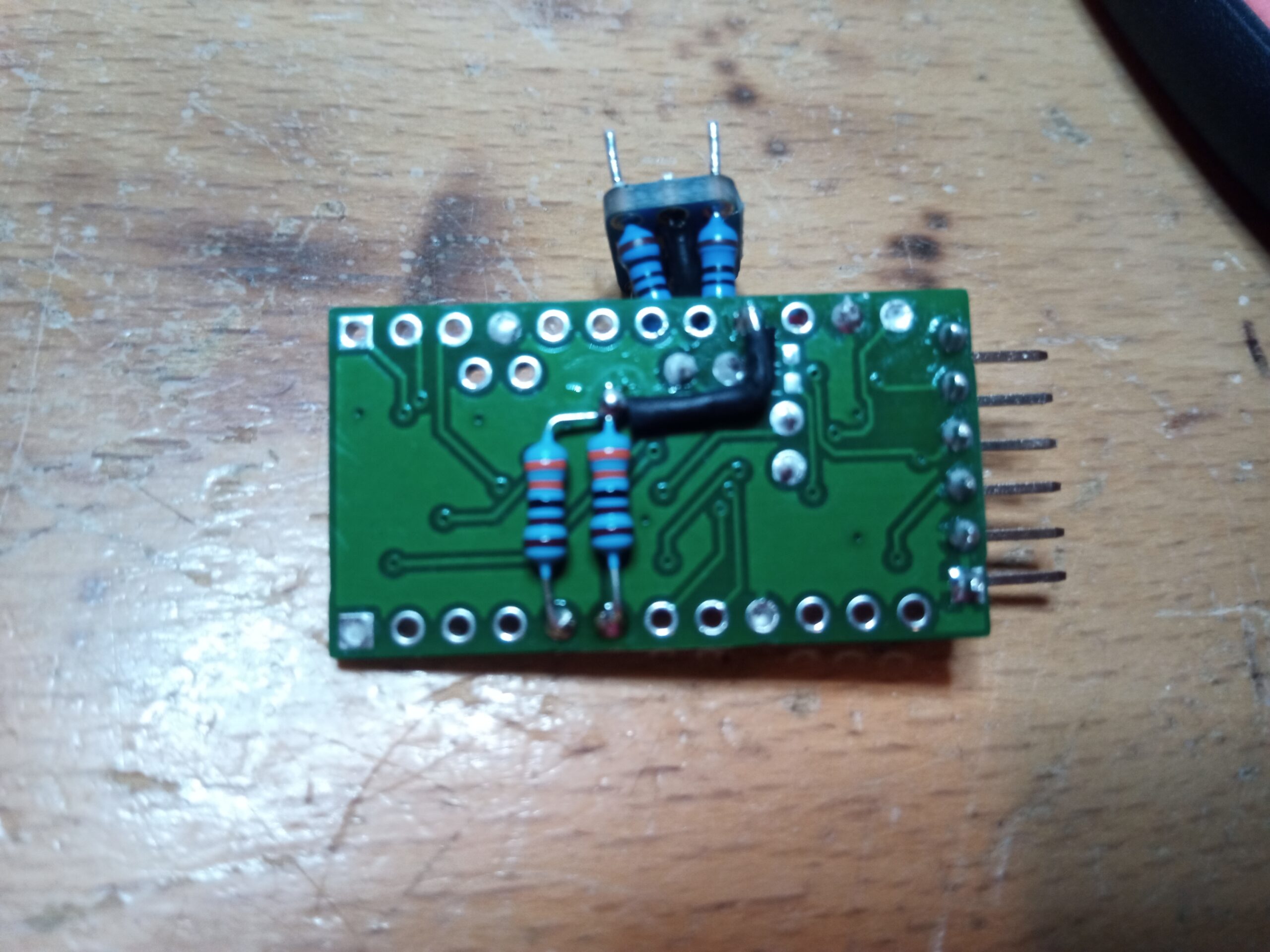
When using the above software, I can recommend using a little “modchip” like PCB I created, which contains all the components for the mod, sans the two 100R I2C resistors which need to go as close to the jungle as possible. Find the Kicad project here.
Note: When I did the initial mod, I was using normal unshielded wires, and I had two vertical lines on the screen. After changing to shielded cables this went away. Another user reported the same thing, but seemed to get them away by changing the routing of the cables. In any case, I recommend using shielded cables to avoid issues.
