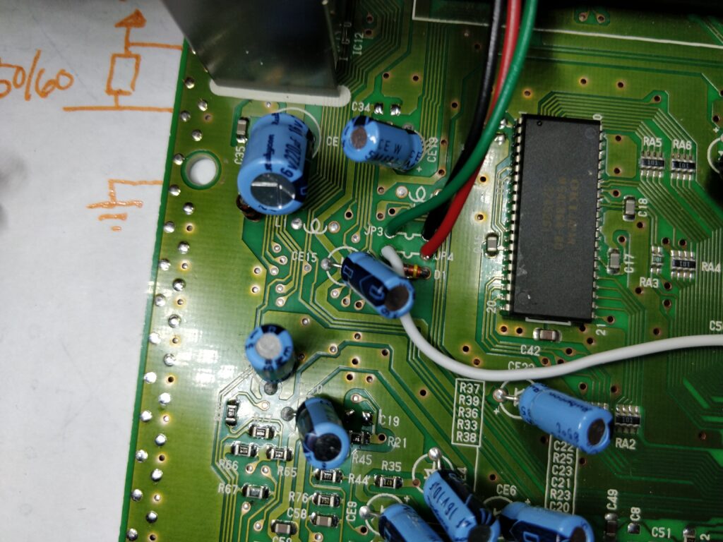
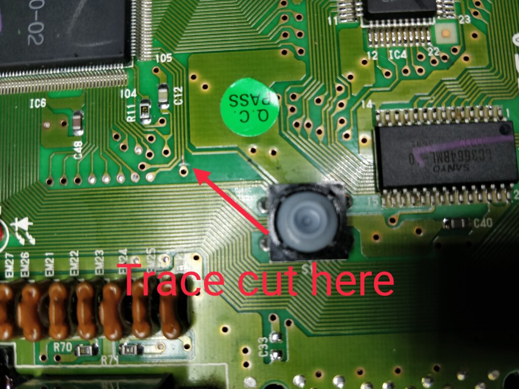
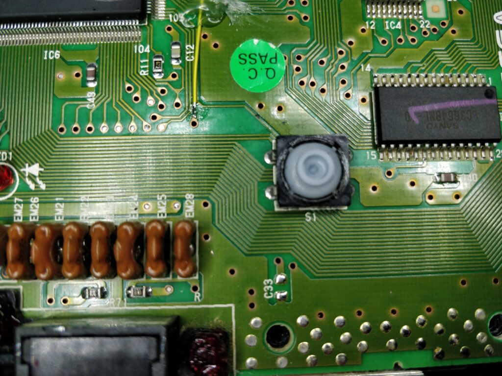
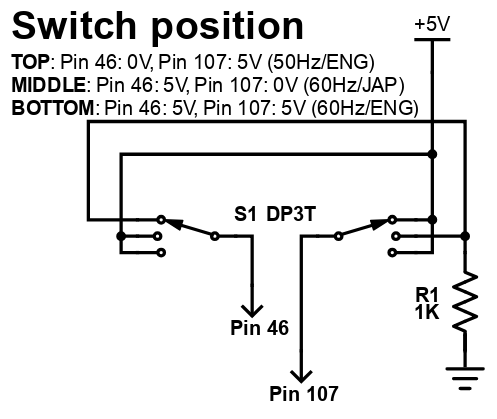
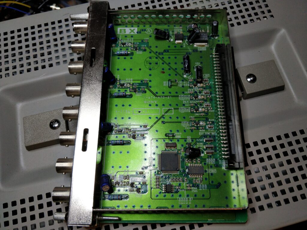
So I got a couple of PVM-9L2’s, both coming with the BKM-120D SDI card, but no analogue RGB inputs are present by default. They can be had by changing the BKM-120D with a BKM-129X card, which supplies standard RGBS/YPbPr in/out BNC sockets. The board is rather expensive, going in the $150’s range on eBay, although not that rare as such. The same board is used in other BVMs and some other PVMs can also use them, if not to add even more RGB inputs.
Anyway, looked into if it was possible to make a clone of it, so I looked at the service manual, and could see that it was more complex than for instance the JVC card (IF-C01COMG) I cloned some time ago.
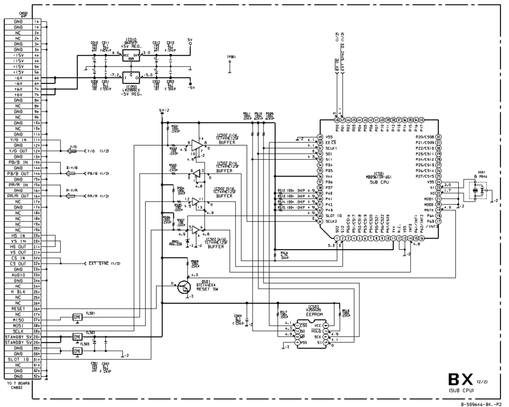
It actually has a microcontroller/MCU on board, coupled to the monitor through the 64-pin socket, seemingly communicating on a SPI channel. SPI usually has 4 wires: a clock (SCLK), data master->slave (MOSI, master out, slave in), data slave->master (MISO, master in, slave out), and a slave-select (SS, meaning “selecting” the slave for communication, usually active low). So two data channels in each “direction” means SPI is “full duplex” which again means that data is flowing in both directions simultaneously (look up SPI on Wikipedia if you don’t know it). Slave-select is not present by default, but there is a SLOT ID pin going from the socket and into the MCU at two places, one called INT0, which is an interrupt pin, and another also called SLOT ID, so I guessed this to be functioning as slave select.
This data channel is then used by the monitor to verify the board is there and read some information from it and so on, thus activating RGB/YPbPr on said monitor, when the card is present (and selected). If the card supplies YPbPr or RGB is then setup in the monitor itself through the OSD, and there is also a serial number readout. At the same time, the microcontroller also has two “digital” outputs, one actually enabling the video output of the card (BX_OE, active low), and one (de)selecting external sync (EXT_SYNC_OE, active low).
To get anywhere I needed to get a card, so I bought one on eBay at too much money (the one shown in the beginning), which further fueled my desire to reverse engineer it, both for myself and the community.
The MCU of the board is some 8 MHz proprietary thing, and it has an EEPROM next to it, most likely with the program of the MCU on it, but since the MCU is not something easily bought, I didn’t try to read it out.
I expected the initialization sequence to be something like:
1. Monitor selects the card by setting SLOT ID to LOW.
2. Monitor reads some info including serial number.
3. Monitor decides card is there depending on response.
4. Monitor starts using card, sends commands commands to turn on and off the output and the external sync depending on button selection.
And then following commands for external sync and whatnot being something like:
1. Monitor selects the card by setting SLOT ID to LOW.
2. Monitor issues some “simple” command.
3. Monitor deselects card.
So to figure out the what commands look like, what response to give, and timings, I attached a logic analyzer to the RESET pin, MOSI, MISO, SCLK, SLOT ID, BX_OE and EXT_SYNC_OE pins. I have a DreamsourceLab DSLogic Plus USB logic analyzer, which can capture for a long period of time which is great, as I need to capture during the whole startup and initialization of the monitor to catch the information (which is around 5 seconds). At the same time, the software for it (DSView) also has built-in SPI decoding, so it can show me the byte representation of the data being transmitted over the wires. The connector is a DIN-41612 style a+b connector, where the bottom row is the a row, and the top is b. Pin numbers are counted from left to right. When the connector is vertical like it is positioned in the monitor, the leftmost column is then a row and rightmost is b, and pin numbers are counted from top to bottom.
So I set up the logic analyzer to capture for 5 seconds, and at 10 MHz (as SPI is often in the 1 MHz range this should be plenty oversampling). So doing this yielded a datastream like this CSV shows:
Complete CSV file of power-up sequence, card selected, external sync on.
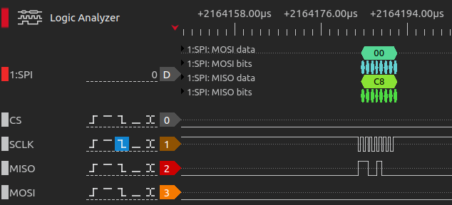
Now SPI actually has 4 possible modes, which will influence how data is interpreted: clock polarity (CPOL) and when to sample the data (CPHA), both can be 0 or 1, thus 4 possible configurations. So to figure out if the representation of the data is correct, these need to be setup properly. First of all, it can be seen that the SCLK is high when nothing is happening/idling, meaning CPOL should be 1. To decide if CPHA should be 0 or 1, you need to look at the transitions of SCLK and the data lines in relation to each other. I decided CPHA should be 1 based on the waveform, meaning data is sampled on the rising clock edge. I then did this multiple times, with different sample speeds also, to confirm I got the same readings again and again.
The output shows that SLOT ID seemingly *is* used as a slave select, the monitor then issues a 0x9E command, the slave responds with the same, while the master seems to clock in an address byte, which then is responded to from the card with whatever that address contains. This is a “classic” memory read pattern. There also seems to be a 0xBE request, which also throws out some data, so I expect that it’s another memory region that is requested or something like that. It then has some 0xF7, 0xF6 and 0xF4 requests, which seems to be depending on if it is selected, and if external sync is enabled or not.
My current idea of the protocol is then like this:
0x9E – Memory read (followed by an address to read).
Example: 0x9E, 0x02, 0x00 reads memory address 0x02 (the last 0x00, is where the master clocks out the response), so response would be 0x9E, 0x39.
0xBE – Memory read of “another” region (followed by an address to read).
The next here are preceded by 0x00, 0x00:
0xF7 – Deselect (turn off outputs).
0xF6 – Selected, output enable (BX_OE=LOW/0), external sync disabled (EXT_SYNC_OE=HIGH/1).
0xF5 – Also some deselect, see it rarely.
0xF4 – Selected, output enable (BX_OE=LOW/0), external sync enabled (EXT_SYNC_OE=LOW/0).
Upon startup, the card always gets two deselect (0xF7) and then a one of the select commands, depending on the external sync state.
So my first attempt was simply implementing all this in an Arduino Nano, putting the protocol into a request/response state machine, that each time the monitor asked for a specific byte, would return the same as the original BKM-129X did. This proved not to work. I got the request, 0x9E, and it was sent back, but then SLOT ID goes HIGH, and never LOW again to read the response. Hot damn…
So I looked some more at the waveforms, and noticed that the same happens for the original card, however SLOT ID goes LOW again some time after the 0x9E response, and then stays LOW for quite some time, until SCLK suddenly starts clocking in the response data. Since this was not happening on my setup, I thought that maybe this was some part of a handshake, because of the SLOT ID labeled pin on the MCU itself. So my guess was that the MCU should slave-select itself when the actual response was required, sounds somewhat strange, but hey, it’s Sony. And whaddayaknow, it worked!


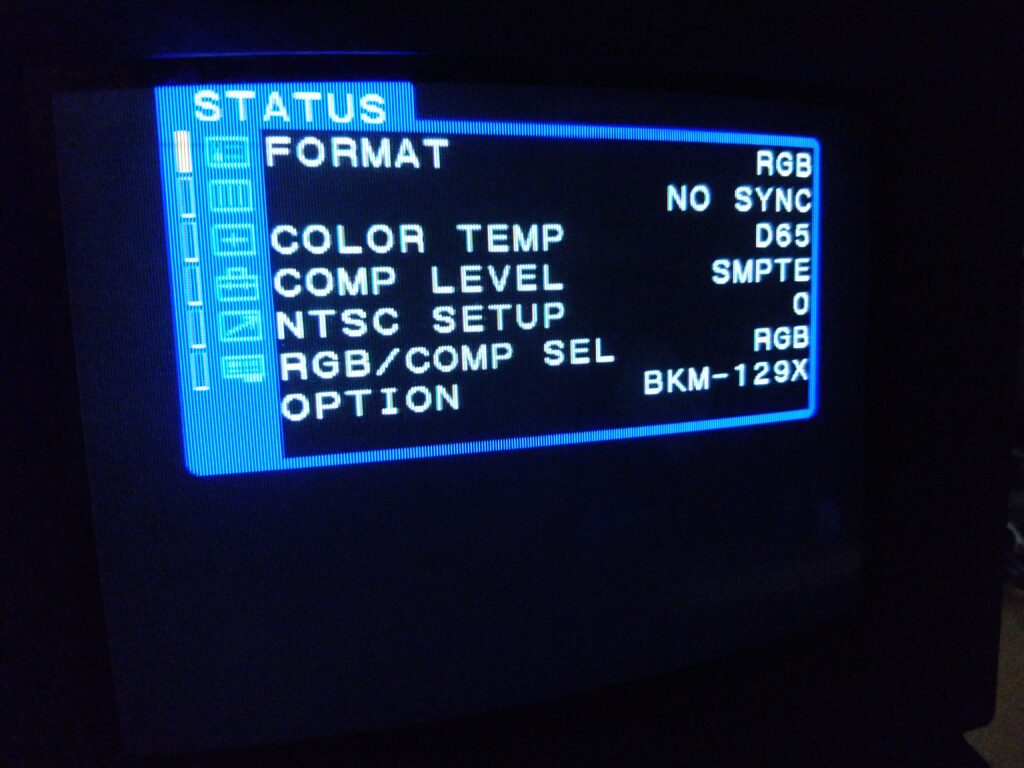
Doing this, I could now, having only the Arduino Nano connected, select RGB (no picture of course), read out a serial (that was identical to my original card) and select and deselect external sync. So to do it, SLOT ID pin is first configured as input, and when the actual response is needed, it waits for the SLOT ID from the monitor to go HIGH, then the pin is configured as an output, output is set LOW (thus slave selecting itself), waits for the response to be read out over SPI, and then it sets SLOT ID as HIGH, and back to an input.
Now I have no idea what most of the data reads represent, except it seems (at least) the first byte read, address 0x00, returns 0xC8 for the BKM-129X and 0xC0 for the BKM-120D, so I expect this is what the monitor uses to identify the card. The next addresses read, 0x02-0x09, represents the serial number, written in ASCII bytes (so 0x30 for 0, 0x31 for 1, 0x32 for 2 and so on, www.asciitable.com). Looking at the CSV from earlier, it can be seen that my original card has the serial number 2001911 (0x32, 0x30, 0x30, 0x31, 0x39, 0x31, 0x31).
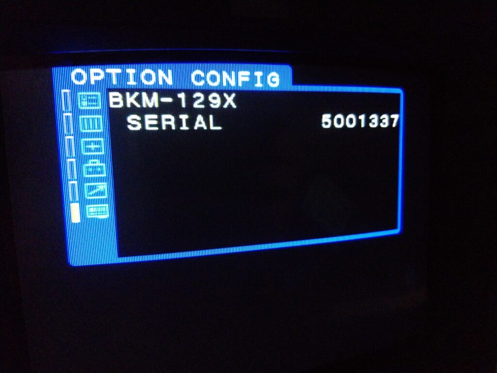
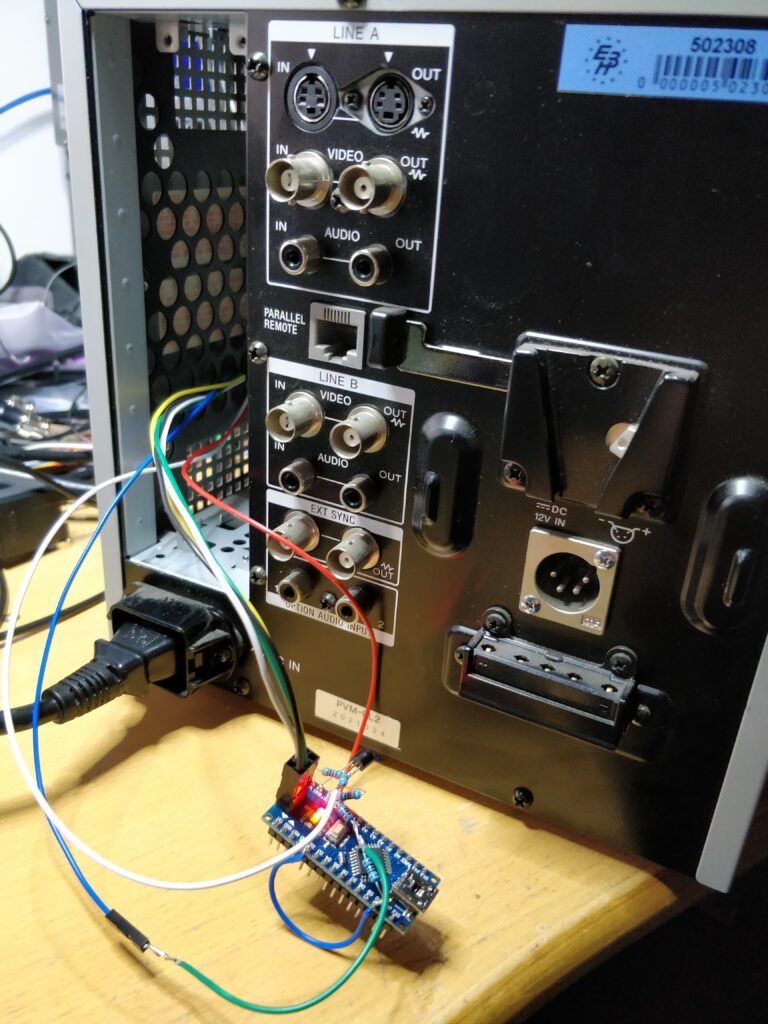
I’ve put the code, which works on an Arduino Nano v3, on my github: https://github.com/skumlos/bkm-129x-mcu/
Update
So since the code now has been refactored and changed a bit, and tested on more monitors, at least newer monitors like the BVM-D9H and D14H seem to require that the bootloader is removed and the application is running as the only piece of software (seemingly to boot faster). This can be accomplished by programming the software directly to the Arduino, without using the USB. This means a “real” programmer (ISP) is needed, and the ICSP header (or the corresponding pins) are used for programming. A cheap ISP can be made with another Arduino Nano, check out how to do that here: https://immerhax.com/?p=480 (scroll down a bit)
Any feedback is appreciated, please email to martin@hejnfelt.com or reach me on shmups (username: skum), on the CRT discord (username: skum) or on Facebook (Martin Hejnfelt).
Next up is designing the rest of the board to have a true compatible card. I am in the last stages of this, and will release here and github when done.
