TL;DR Change the corresponding (or all three as I did) SOT-23 MOSFETs closest to the LED strip connector wires on the “mainboard”. ATTENTION Mind the infinitely small resistors right by pin 1 and 2 of each MOSFET!
My daughter bought two TP-Link Tapo L900-5 Smart LED Strips, which can be controlled by her phone. One of them suddenly constantly showed blue color, always, even when turned off. Googling the issue, it seems to be a quite common issue with the very inexpensive LED strip, sometimes only happening after a few months. Sometimes it’s one of the other colors that’s constantly on or a color doesn’t work or whatever. Anyways, on to fixing it…
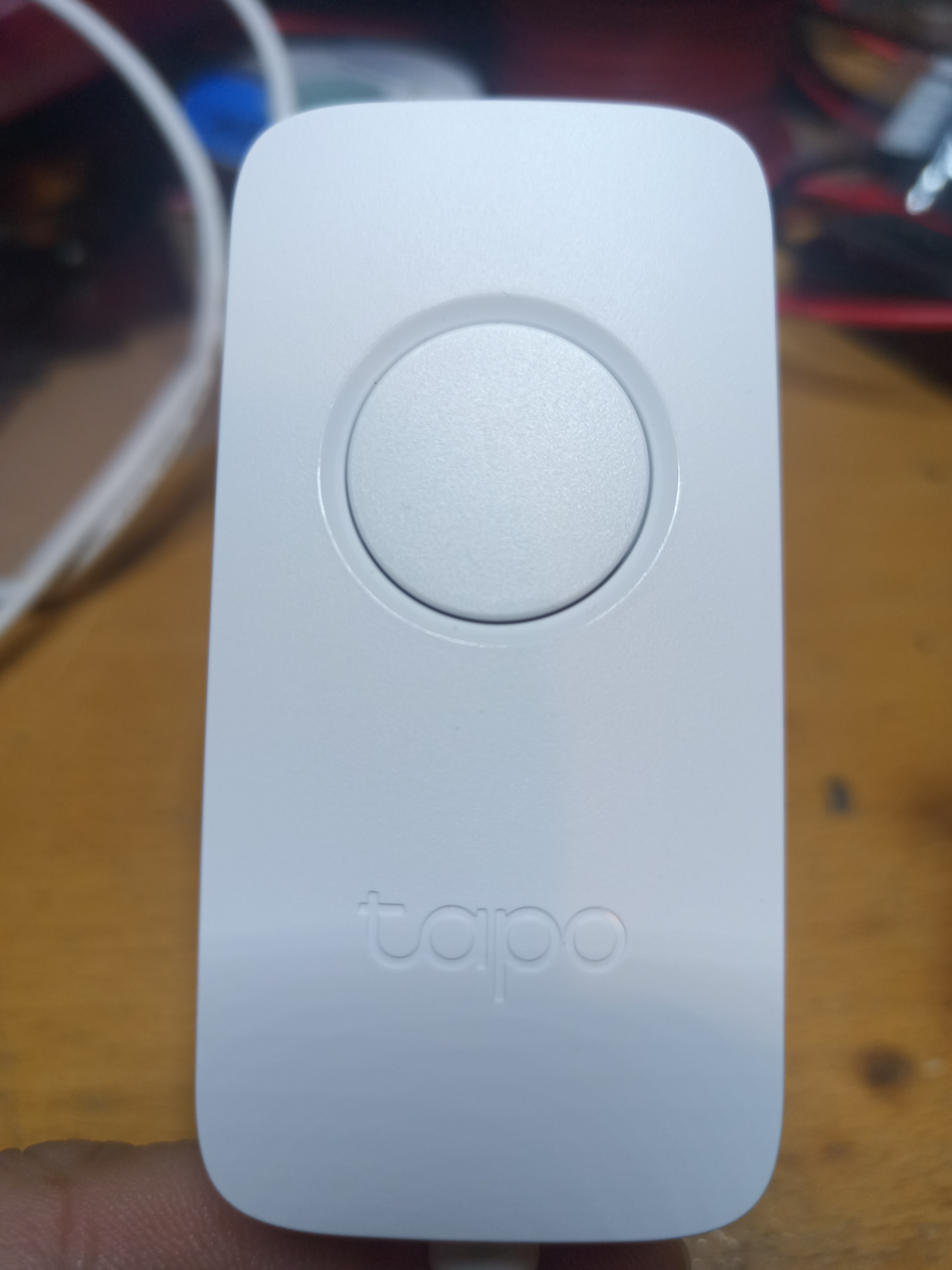
The Tapo L900-5 main unit
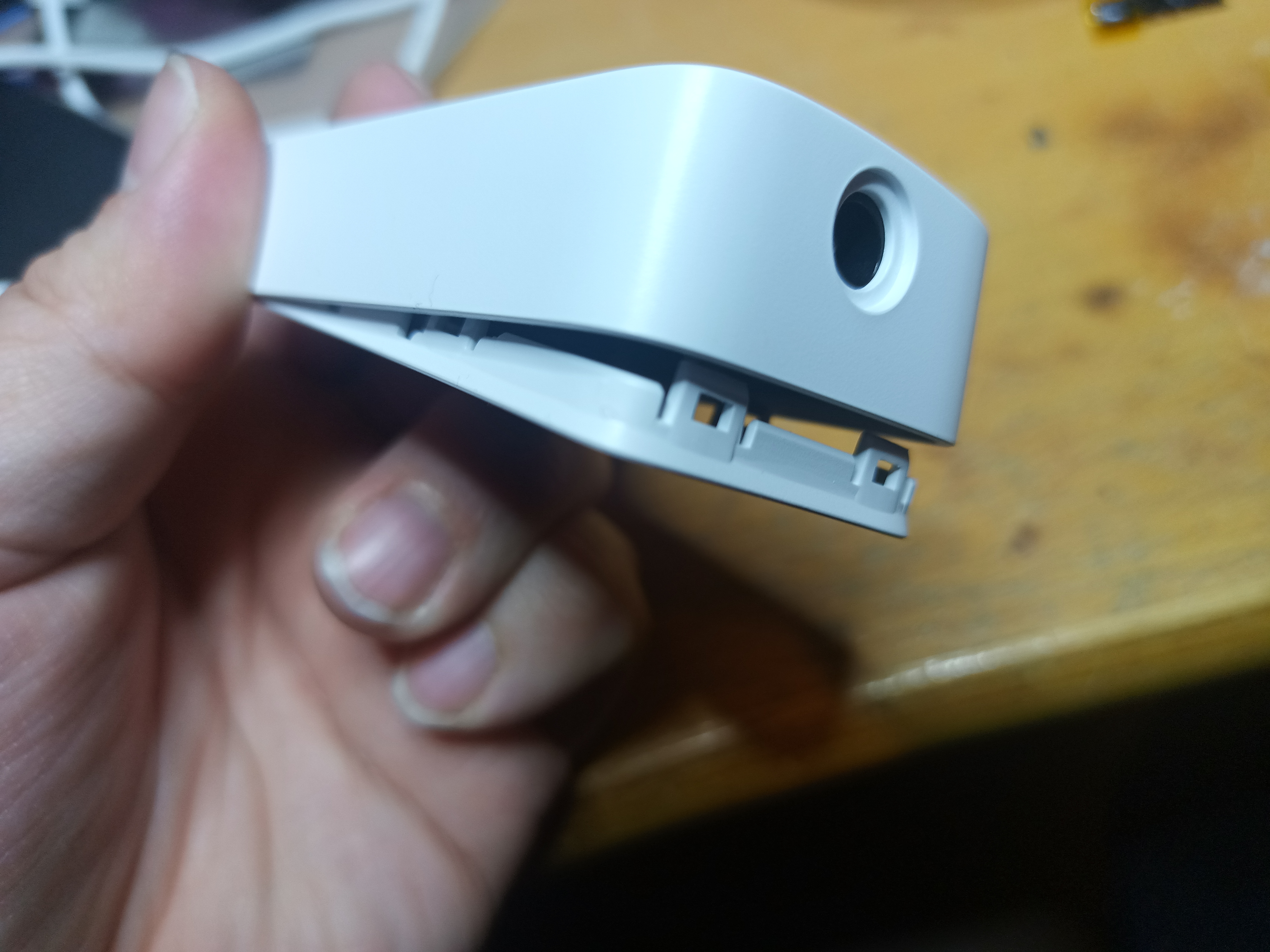
Anyways, I thought I’d see if I could fix it, so I opened up the main unit. It disassembles pretty easily by simply prying around the edge with a flathead screwdriver or similar unit. I have like this thin metal thingy from a phone fix screwdriver set which opened it like a charm.
The bottom is easily removed…
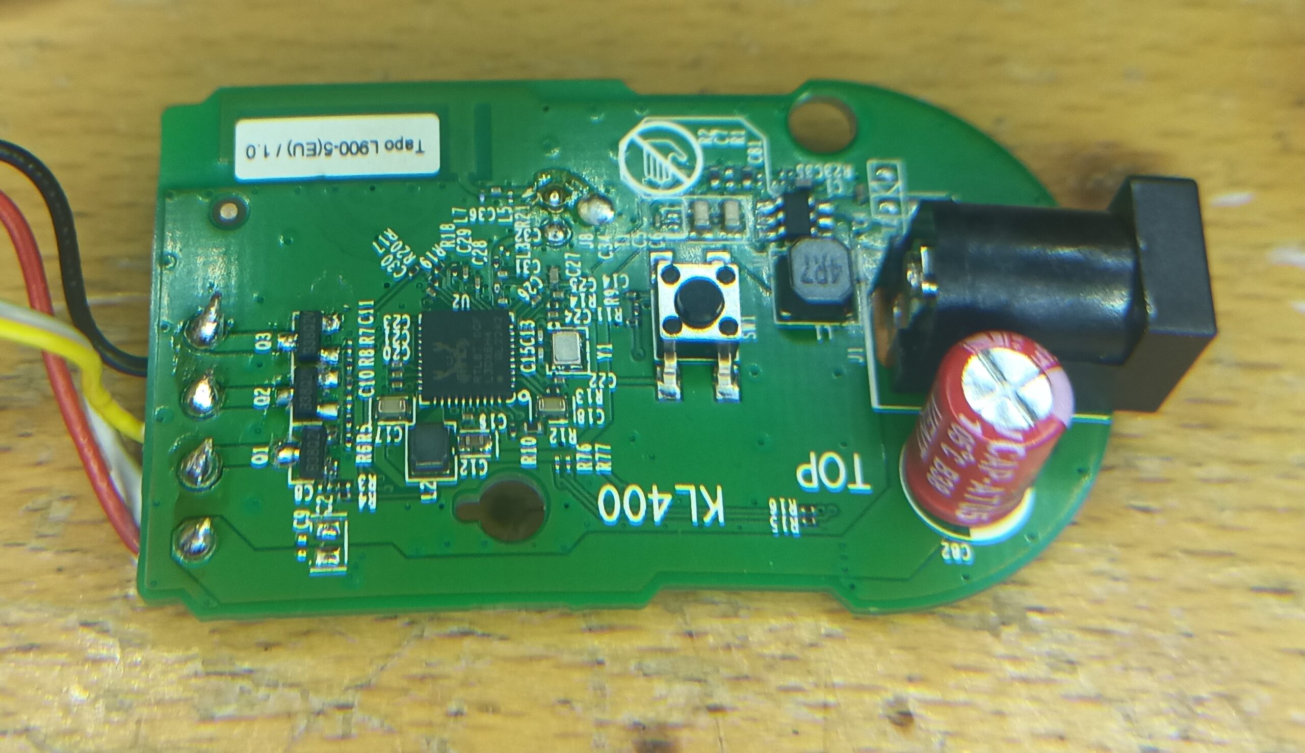
Inside is a small PCB which essentially holds some regulator stuff and the Realtek something something chip that most likely is some off the shelf LED strip controller with WiFi and whatnot.
The Tapo L900-5 mainboard
Now don’t mind the red capacitor. I have a knack of replacing caps in stuff, because I’ve had so many various small units die, then I replace a single cap or so, and then they spring back to life. Anyways, what interested me were the three SOT-23 units to the far left.
Since it was just one color that was constantly on in this case, I thought maybe these guys were transistors or MOSFETs and that they each controlled a channel in the RGB LED strip. I tried de-soldering one and testing it on my BSIDE ESR02 Pro thingamabob-tester, and it showed this:
This lil’ tester thing, is awesome!
So hooray, it was a MOSFET, and testing the one going to the B channel of the strip (in this case it’s the top one) the meter just showed a resistor, so conclusion, the MOSFET had died. I guessed that this unit isn’t particularly picky with the specifics of the MOSFET, except it of course needs to have a drain-source voltage of at least 12V, as that’s the LEDs working voltage, I found a pair of BSS138 MOSFETs and replaced all three (which I managed to do quite crookedly, as can be seen on the pictures above, where that has already been done). Presto, unit now works again 🙂
ATTENTION! Please observe that right in “front of” the MOSFETs (so to the right on the pictures above) are some small resistors in like 0201 package or something. Do *not* put your iron on those guys for long, otherwise you might remove them, and then all hell’s loose, as you don’t wanna hand solder those suckers back if you can avoid it :).
Update: This has been confirmed to work on a Barco ADVM 28 also
Note: This was originally only targeted the ADVM14. As time went by I’ve modded all but the ADVM28, and added info here, which may make it seem a bit confusing read. Sorry 🙂
The Barco/BarcoNet/Scientific Atlanta ADVM line (ADVM10/14/20/28) is notorious for its weird selection of inputs. Two composite, S-Video and SDI, but no component/RGB, makes it somewhat unfavorable for many CRT enthusiasts, so RGB modding it has been on the list for many. Many of the previous mods, at least the ones I know of, revolved around hijacking the SDI input and using a RGB->YUV converter. This seems to work with various success, depending on the version of the monitor seemingly, again I am not an expert on this brand or unit, but since the unit has no less than 2 jungle ICs, and one has two unused RGB inputs, I thought that was the way to attack it instead. I am unsure of how much the various versions of this monitor differ, mine is BarcoNet branded.
Update: So it seems there are multiple “generations” of the Barco ADVM monitors. The early (around 2000) units (at least of ADVM20/28) “only” have a single composite channel, S-Video and SDI with no passthrough. I have modded one of these using the same method, and it works fine. To avoid losing composite/S-Video, I chose to use blanking from SCART instead of from the Arduino.
Now the “secondary” jungle is the one dealing with S-Video and composite, a Philips TDA9321H. This unit has two unused RGB inputs, RGB1 and RGB2, where RGB1 can be converted to YUV at the same time, so some form of YPbPr should also be possible. That road is yet unexplored. I chose to start out with RGB2 to risk the fewest issues to begin with.
The TDA9321H
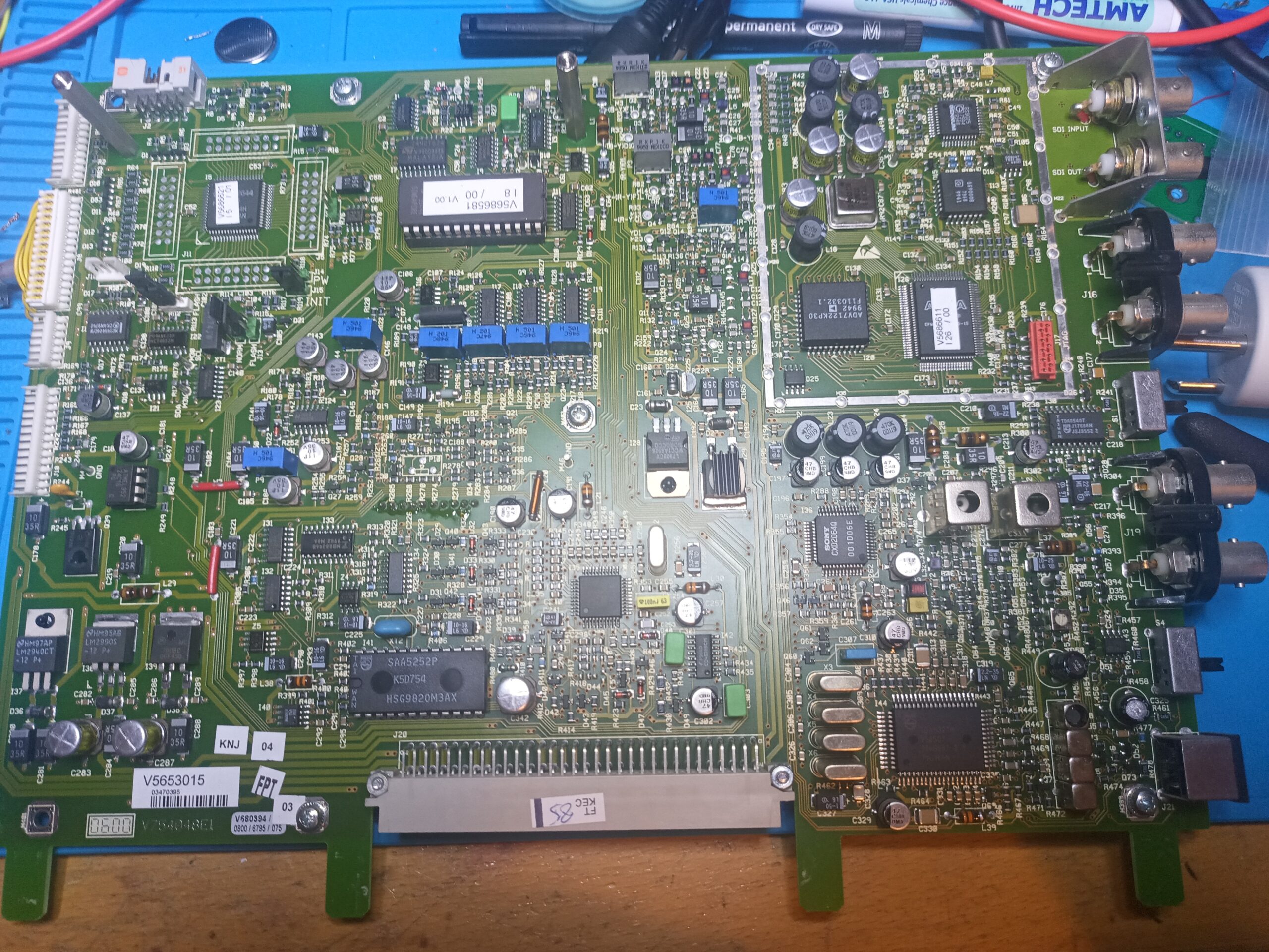
The signal board that needs to be worked on is on the back plate of the monitor, so unscrew a million screws and get that board out. When done, you should have this:
Picture 1 – The ADVM14 signal board
Picture 1B – The signal board of the “early” generation ADVM20.
Picture 1C – The ADVM10 signal board, the TDA9321 is in the bottom right corner
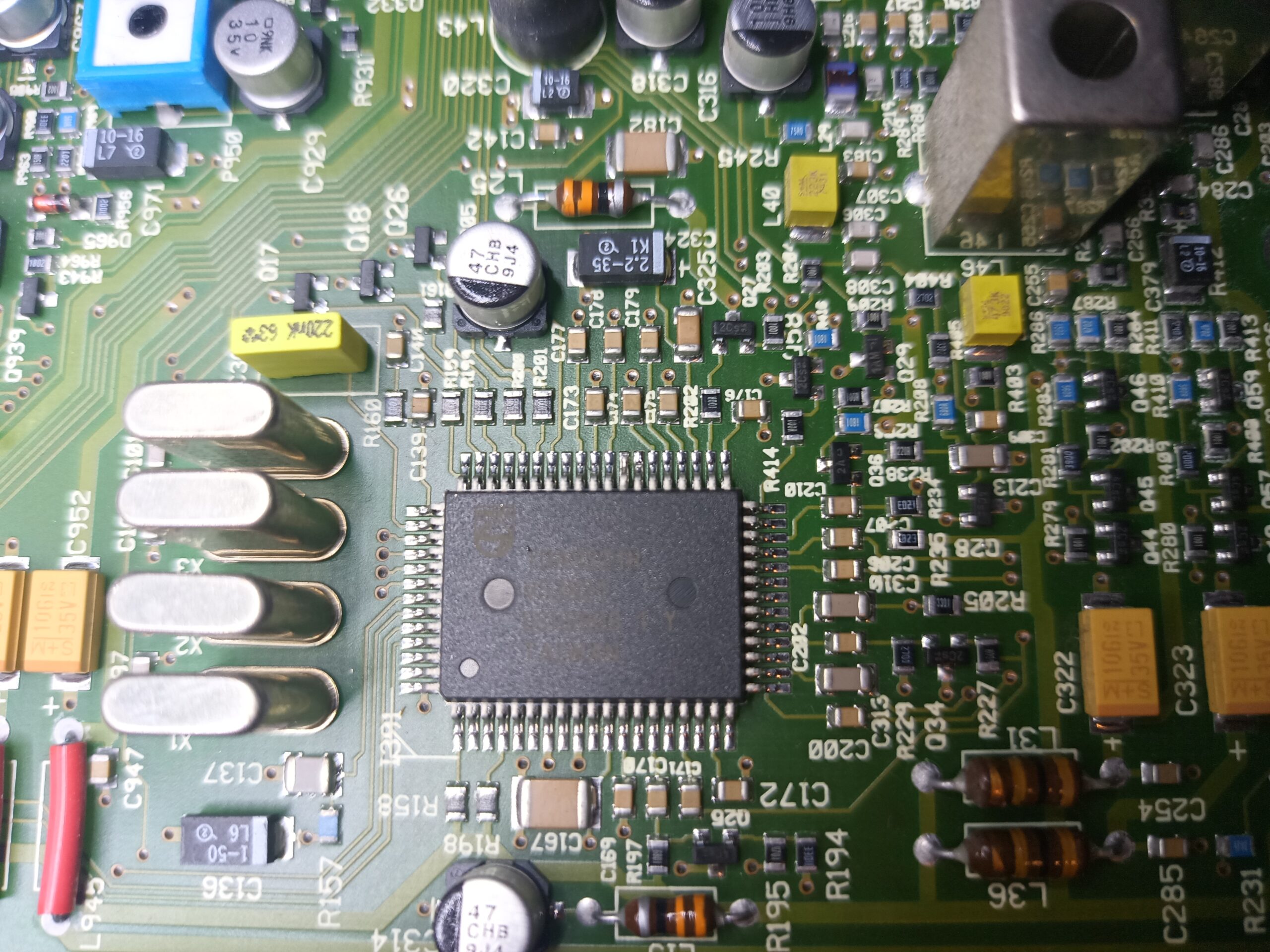
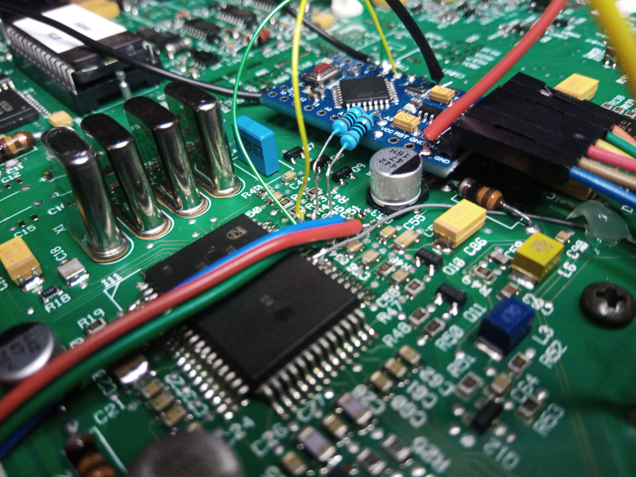
Now the TDA9321 is the one in the middle left (I put a sticker on here with some lines showing the pins) its reference is I11.
Picture 2 – Closing in…
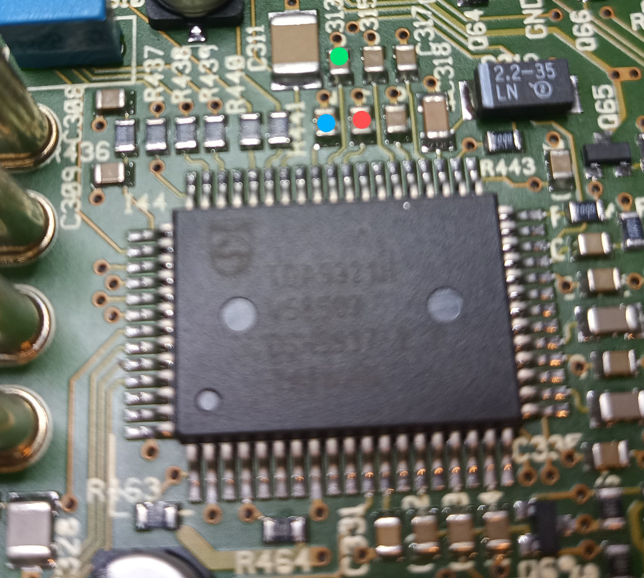
Picture 3 – The thing! The black line is NOT GND 🙂 The RGB lines are in front of BI2 (43), GI2 (42), RI2 (41) and the longer orange line is RGB2 (40) which is the insertion/blanking pin for RGB input 2.
Picture 3C – Here is the “early” generation circuit. The resistor and capacitor references are different.
ADVM10: Capacitors and resistors are named different, but are placed kinda like the others.
Now firstly, I verified with a logic analyzer that the RGB inputs really were disabled in software, and sure enough, the tenth register, 0x0A is constantly written as 0x00. Here are the values that are constantly sent to the monitor, first is the hex address, next is the hex value, last is the value in binary:
If we check the datasheet, this means the following:
Table 2 of the datasheet. Bits are D7-D0 from left to right, meaning we’re interested in at least IE2 and/or IE1, so bit 1 and 0.
At the same time, RGB1 (and RGB2) are both directly connected to GND (no pulldown resistor) which means no matter what, we need to lift pin(s) which always suck due to the risk of breaking them.
Another interesting observation is that it does not change the input/output registers (0x08 and 0x09) depending on CODED A or CODED B is selected, which I guess means that the signal is switched elsewhere. It would have been nice to be able to distinguish which signal was selected, but only SDI and S-Video selections trigger actual changes to these values.
Update: So the composite video is switched via a TDA8540 video mux IC (I21), more or less the largest IC to the right in picture 2 above. When CODED1 is chosen, register 0x00 (SWI) is written to 0x80 and when CODED2 is chosen, register 0x00 is written to 0xC0, so OUT3 switches between INPUT1 for CODED1 and INPUT0 for CODED2, and OUT3 is then apparently connected to the jungle (through at least a comb filter IC also, a TDA9181). This does not apply to the early generation ADVMs as they don’t have the TDA8540 and the TDA9181, but instead “just” a Sony CXD2064Q comb filter.
Anyways, first of all we need to renable IE1 and/or IE2. Just as with the JVC monitors that did something like this, the “obvious” choice is to intercept I2C communication and change the data sent to register 0x0A from 0x00 to at least 0x03, as that would set the two lowest bits to 1, thus enabling IE1 and IE2 as per table 27 and 28 of the datasheet:
So just as with the JVCs the jungle needs to be isolated from the I2C network of the monitor. This is done by removing R44 (SDA) and R45 (SCL) resistors which can be seen just above the chip to the left from the previous picture 3. These two are the 100R “termination” resistors or whatever we call them, added to minimize signal reflection and such. I then wrote a small Arduino sketch that makes the MCU act as a middle man, and forward the data from the monitor to the jungle, and back, but changing the 0x0A data to 0x03. You can find the sketch here.
Now I used a Mini Pro board, where the hardware I2C is connected to pins A4 (SDA) and A5 (SCL). Connecting these two pads through a new 100R resistors, connected to the pads farthest away from the chip, will make the Arduino act as the TDA9321H. Now to relay the information back to the original jungle, the sketch creates a “software” I2C master line on D4 (SDA) and D5 (SCL) and we thus need to connect those to the two closest pads of R44 and R45, so it can speak to the jungle. Remember to add pull-up resistors to those two lines, so a 2.2-3.3k from D4 and D5 to the Arduinos 5V pad.
On the “early” generation, the resistors are R200 (SDA) and R201 (SCL).
On ADVM10 they’re R440 (SDA) and R441 (SCL).
Power to the MCU can be taken from the large 7808CV regulator in the top of the board, and feed it to the RAW input of the Mini Pro (or similar if you’re using a Nano 3.0 etc). Same goes for GND, but there are also plenty of large GND pads scattered around the board.
If the Arduino is programmed correctly, you should be able to start the monitor up, connect a composite video signal, and apply 1-3V to RGB2 to see the screen go black (because nothing is input to RGB input pins yet).
Now how the Arduino program works apparently influences a lot how everything goes. I spent some time tweaking it until it now seemingly works, otherwise the screen would start to flicker, tear and seemingly go out of sync. I think this is because of the two I2C lines from time to time influencing the timing in regards to each other, as the MCU is single core, but the current revision seems to fare fine. I am contemplating switching to a RP2040 or similar, but that would then require level translations as the jungle needs at least 3.5V for a high signal, and the RP2040 is a 3.3V system. For now I’d like some feedback as to how the current Arduino method works.
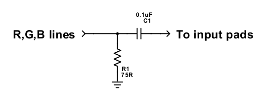
The three color signal inputs are BI2, GI2 and RI2, which are “grounded” through C51 (BI2), C52 (GI2) and C53 (RI2) which are just right of the R44 and R45 resistors. On the early generation these are C177 (BI2), C173 (GI2) and C178 (RI2). These need to be removed, and the corresponding pads closest to the jungle, are where the RGB signals should be connected, through a 0.1uF capacitor, and a 75R termination resistor to GND, like this:
The lifted RGB2 pin, should be connected to a blanking signal between 1-3V. If SCART pin 16 is used, a 75R resistor to GND is advised, otherwise take appropriate measures to create a compatible voltage, eg. through voltage dividing the 8V, so something like a 22K and a 8.2K will give roughly ~2V. Sync should be fed directly to one of the CODED A/B inputs, I suggest CODED A, if you’re using BNC you can just plug it in, if you’re using SCART, solder sync wire to the center pin of the BNC plug on the PCB.
When everything is hooked up, mine looked like this:
Picture 4 – It ain’t pretty but it works. I suggest using hotglue to secure the wires to avoid accidentally ripping traces and pads.
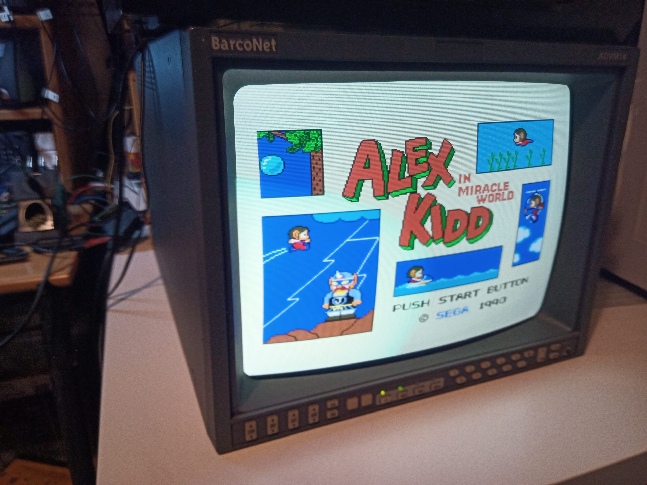
After doing this, you should now be able to input a RGB signal while blanking with 1-3V on RGB2 pin. Here’s the monitor with SEGA Master System 1 connected. The picture’s bottom part blurriness is my phone, not the image of the screen 🙂
So that’s it! Let me know if you try this, and what issues you run into…
Wiring up RGB
So Barco chose this fancy backplate all in metal, which I didn’t want to ruin. There is however an unused DE-9 cutout labelled “RS485”, which I thought would be nice to install a HD15/VGA port in, to avoid any drilling, especially because VGA breakout cables exist in many forms. I thus created a small PCB that can accomodate a HD15 port and the termination resistors plus DC bias caps, kinda like my previous SCART breakout board, and paired with a couple of 7mm M3 standoffs, fit perfectly in the space.
I then wired some shielded 75R mini-coax cables from the board to the input pads, so it looked like this:
The mini-coax is a Tasker C263 cable I split up.
ADVM10 notes: Don’t run the cables over the signal board, but around the *back* of the board, like here. If you run it over, you most likely won’t be able to put the top cover on.
ADVM10: The signal wires run behind the signal board. I guess this makes shielded coax even more important.
For the early generation ADVM, I chose to use blanking from SCART. The HD15 board supports adding a 75R resistor (R21) for HD15 pin and then use this pin as blanking. Then “short” the bottom pads of the footprint for the manual switch like so:
The bottom three pads “shorted” and a 75R resistor on R21 for early generation.
The BLANK(ing) pin from the connector is then wired to RGBI2 pin on the jungle.
Since pin 9 is rarely broken out in HD15/VGA breakout cables, I chose to make a small SCART to HD15 board that runs blanking to pin 9.
Top side of the SCART to HD15 board. RCAs to break out audio from SCART.
SCART block fastened to the HD15 port with UNC 4-40 screws that are approx. 15mm in length.
Find the Kicad project for the SCART-to-HD15 board here: https://github.com/skumlos/scart-to-hd15
Download the 3D printable shell here: https://www.thingiverse.com/thing:6484206
Auto blanking to RGB (only applies to “new” ADVMs)
You might’ve noticed the above picture now has two Arduino Mini Pro’s. This is because the HD15 setup has a “problem” and that is blanking. VGA breakout cables usually just go to 5 BNCs or something, so there is no apparent means of blanking. The 5V/KEY pin of VGA plug, would be obvious, but again, usually not broken out. Also, I still didn’t want to drill the backplate and install a switch.
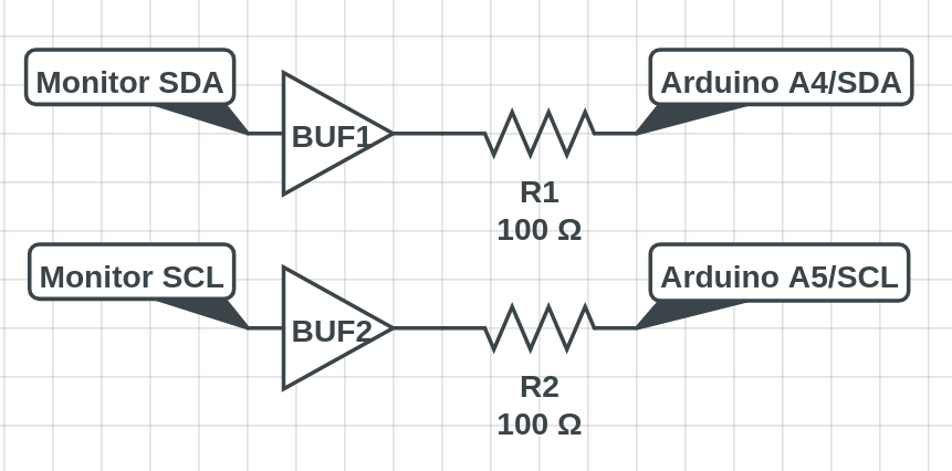
So my plan was to make the monitor automatically blank, when CODED1 was selected. By that I would still have CODED2 for composite and S-Video. Problem is I thus needed a way to know which composite input is selected. There are a bunch of options that makes sense: The TDA9321H has multiple composite inputs, so I actually thought I could simply check which one here, but switching between CODED1 and 2 doesn’t trigger anything. Then there’s a TDA9181 comb filter has two inputs, so I thought the two composite video inputs were switched there, but no. I found out it’s switched in a TDA8540 video mux (I21) as written/appended earlier. This mux has a couple of outputs that *could* have been used to further switch other signals, like audio, but those weren’t used either, so only one thing to do: Intercept the I2C signal to the TDA8540. Problem was then, that when I attached two Arduinos to the I2C line of the monitor, it stopped working. This must be because of the push/pull abilities of the I2C master, and the requirements of the Arduinos I/O pins (at least that’s my best explanation), so I had to turn it into a “sniffer” instead (which is fine, as we don’t actually need to change any data, only listen). So to do this, the second Arduino’s I2C lines A4/SDA and A5/SCL was “prefixed” with a non-inverting buffer and a 100 Ohm resistor like so:
I used a SN74LVC2G34DBV on a small SOT-23 breakout, and then supply it from the Arduino Mini Pro’s 5V and GND outputs. The 100R is to ensure that when the I2C line is released by master (and thus pulled-up) then the Arduino’s ACK part of the I2C communication protocol (where it pulls the SDA line low) won’t “short out”. Thus a 1K or similar might be just as good. The Arduino then pulls its D13 line HIGH when CODED2 is chosen, and LOW when CODED1 is used. This signal is then passed onto the other Arduino which then based on the video switch signal blanks if composite is selected *and* CODED1 is selected. Blanking pin is D13 in the TDA9321H, and the 5V output of the pin is run through a voltage divider consisting of 2x1K resistors, so the resulting 2.5V is used as the actual blanking signal. I put the Arduino sketch for the TDA8540 sniffer here: https://github.com/skumlos/tda8540-sniffer
Update: Doing it with a single MCU
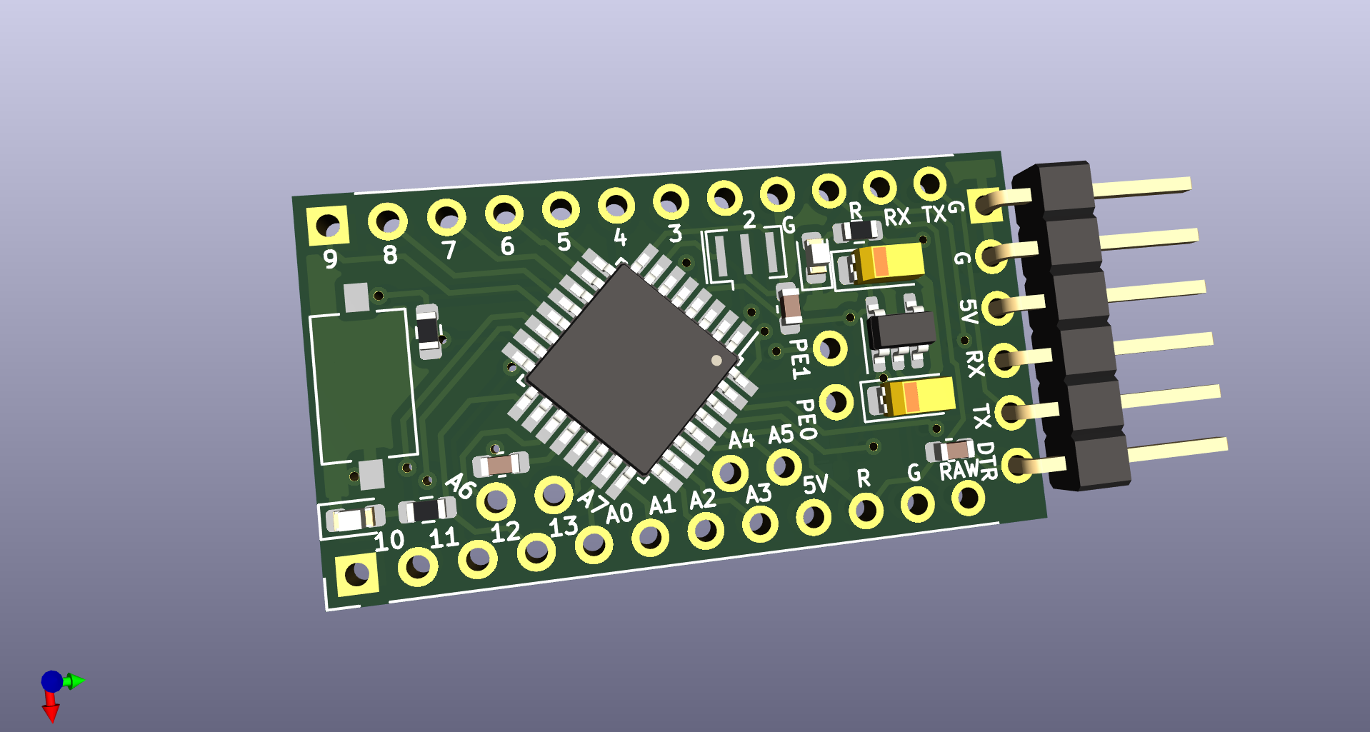
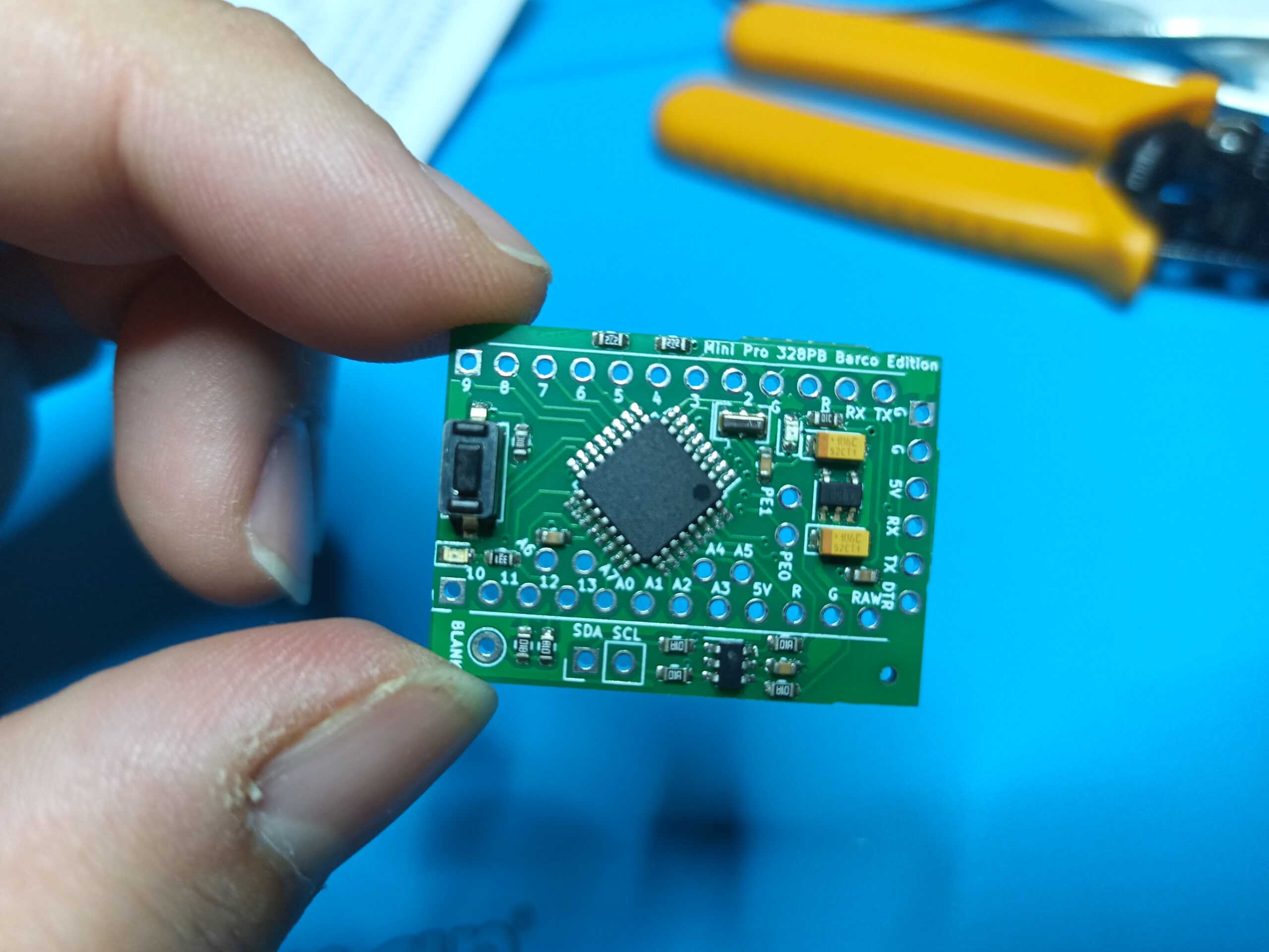
I really don’t dig the two Arduinos, so I made a “clone” of it which uses the ATMEGA328PB as it has two I2C ports. PE0 is SDA1 and PE1 is SCL1. Note that to use it, you need support fore Wire1, which can be found in MiniCore board support in Arduino IDE.
The Arduino Mini Pro clone with a Atmega328PB instead of the Atmega328P MCU.
You can find it here https://github.com/skumlos/atmega328pb-nano It includes direct JLCPCB production files. Remember that when you get these, you need to program fuses and bootloader in. I use an Arduino Nano 3.0 which has been made into an ISP. You can find more about doing that in one of my other posts.
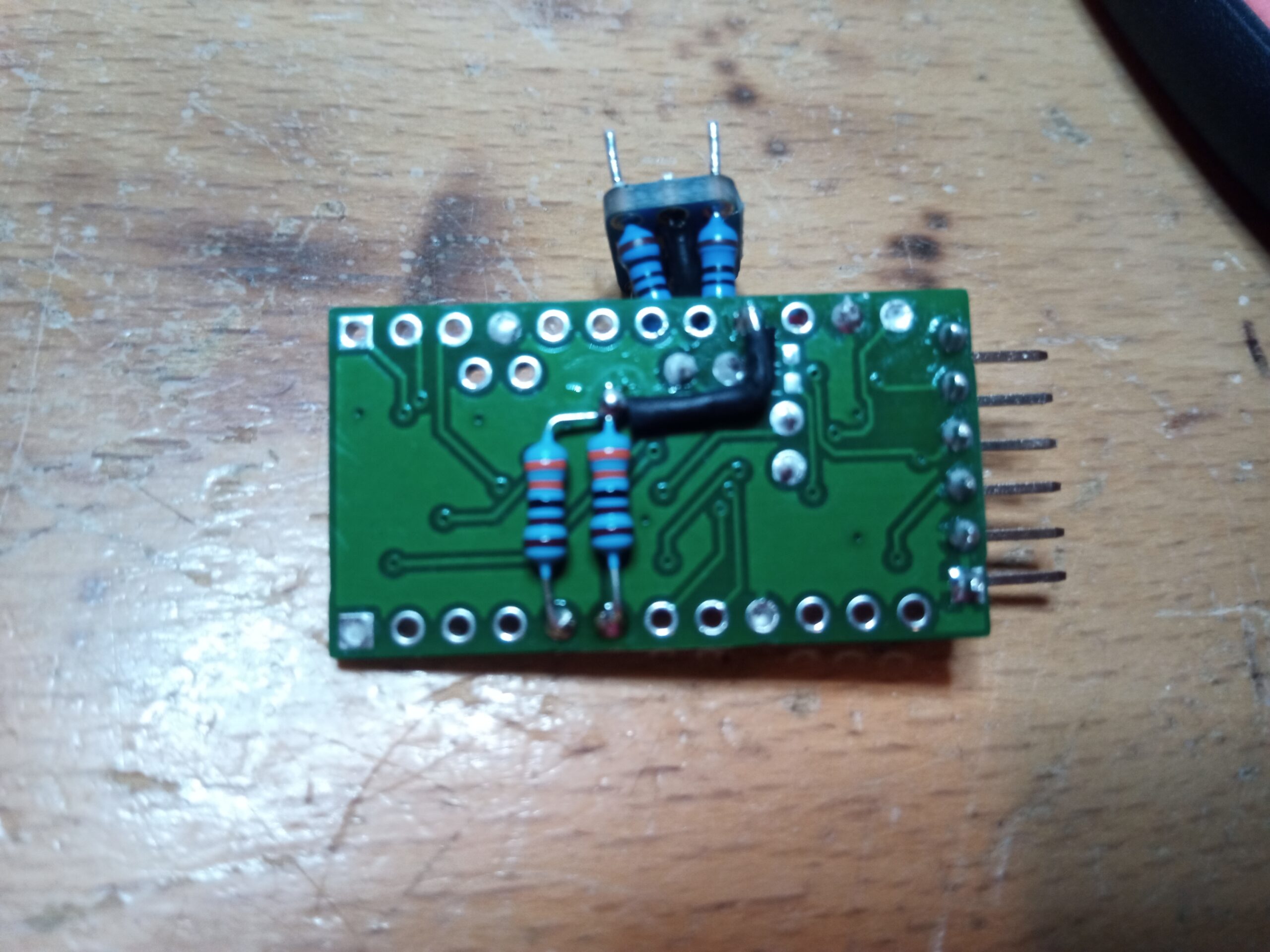
Anyways, just as with the two-board solution, this still requires non-inverting buffers and resistors on the second I2C line, so I used the same SN74LVC2G34DVB on a SOT-23 breakout. The monstrosity looks like this:
The Mini Pro 328PB clone with the buffer on breakout, 100R resistors on I2C and a voltage divider for blanking. Sorry for the blurry picture.
The backside pull-ups on the I2C line for the TDA9321H. Here I used 3.3K. Blurry…
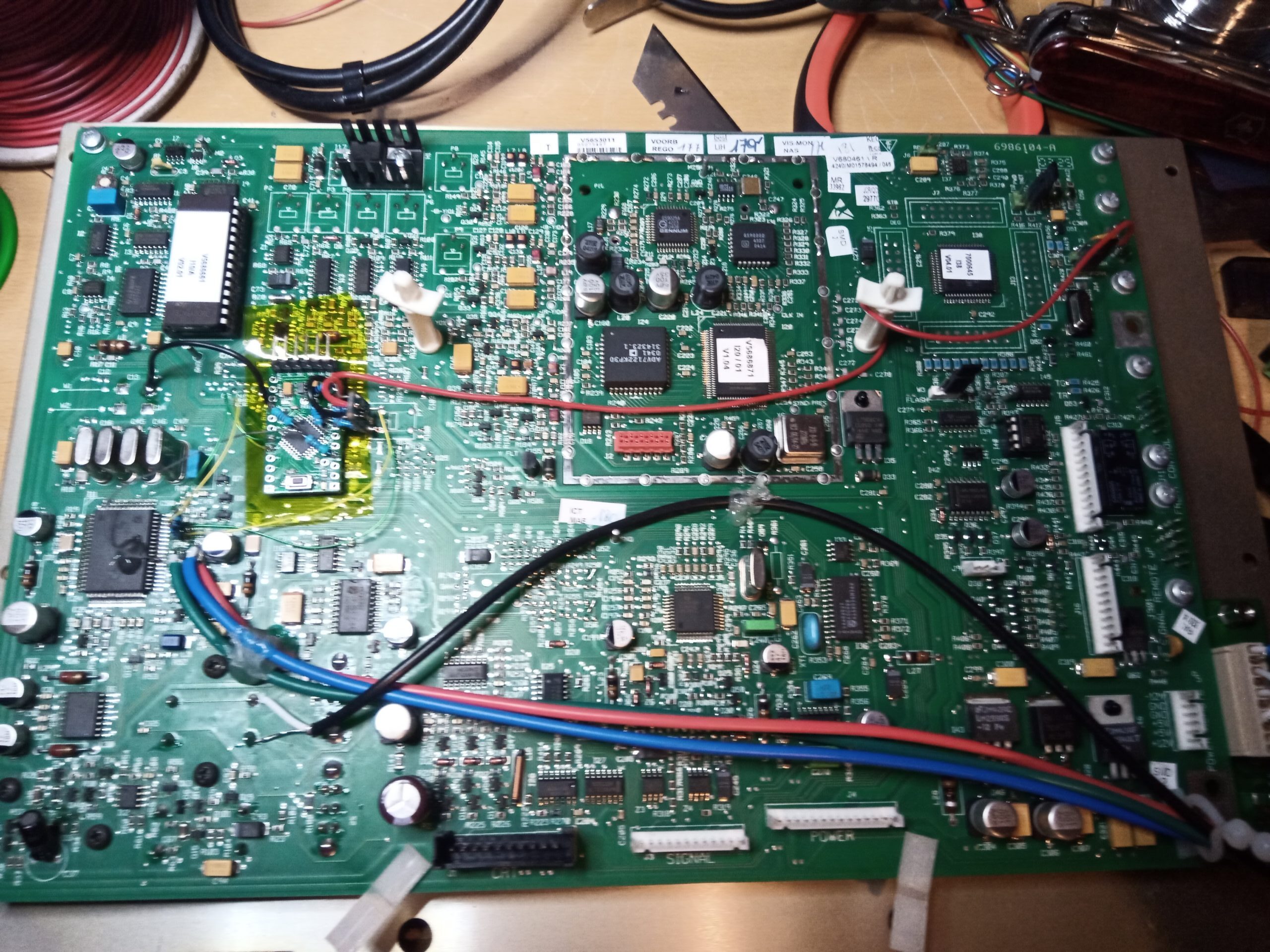
I really gotta take better pictures, but anyways, here it is. I ended up taking 12V from the top connector in the right side, as the 8V regulator gets pretty hot by itself…
So the Mini Pro 328PB Edition requires a “new” program, which is essentially a unified version of the two earlier mentioned sketches. You can find it here: https://github.com/skumlos/barco-advm-bridge
If you use this software for the newer Scientific Atlanta versions, you need to uncomment the “#define SCIENTIFIC_ATLANTA (1)” line. For ADVM10, uncomment the “#define ADVM10 (1)” line.
When using the above software, I can recommend using a little “modchip” like PCB I created, which contains all the components for the mod, sans the two 100R I2C resistors which need to go as close to the jungle as possible. Find the Kicad project here.
Note: When I did the initial mod, I was using normal unshielded wires, and I had two vertical lines on the screen. After changing to shielded cables this went away. Another user reported the same thing, but seemed to get them away by changing the routing of the cables. In any case, I recommend using shielded cables to avoid issues.
Diagram of the connections to the Arduino Mini Pro PB Edition
When building my BKM-68X alternative boards, I’ve been using efinix’ Trion FPGAs which are still fairly new to many. Efinix have been so kind to have the “official” supported programmer be the easily available FTDI chips FT2232H and FT4232H, for which some rather cheap development kits exists, namely the “ft232h mini” and “ft4232h mini” modules. Note that these also exist in a “-56Q” version, which is a bit easier to get going with as some common connections has been done directly on the boards, which is otherwise necessary to manually make.
The non “-56Q” versions seems dead when connected to your PC if nothing is done, but this is simply because the board has options as to how the chip should be powered. Reading the manual of the respective boards should show this:
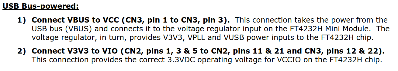
Taken from the ft4232h manual, it is the same for the ft2232h version
So put a jumper (wire) between CN3 pin 1 and 3, and your PC should now actually detect stuff, and then do the V3V3 connections for CN2, as CN3 isn’t relevant for this.
On the Trion based 68X boards there are both JTAG (J401) and SPI programming (J601) headers. The SPI one is the relevant, as we’ll program the SPI flash through this which in turn will be read by the FPGA for its configuration.
The hookup of the programmer is straight from efinix’ documentation:
Taken from AN006 – Configuration of Trion FPGAs
It is recommended to read efinix’ documentation for further information.
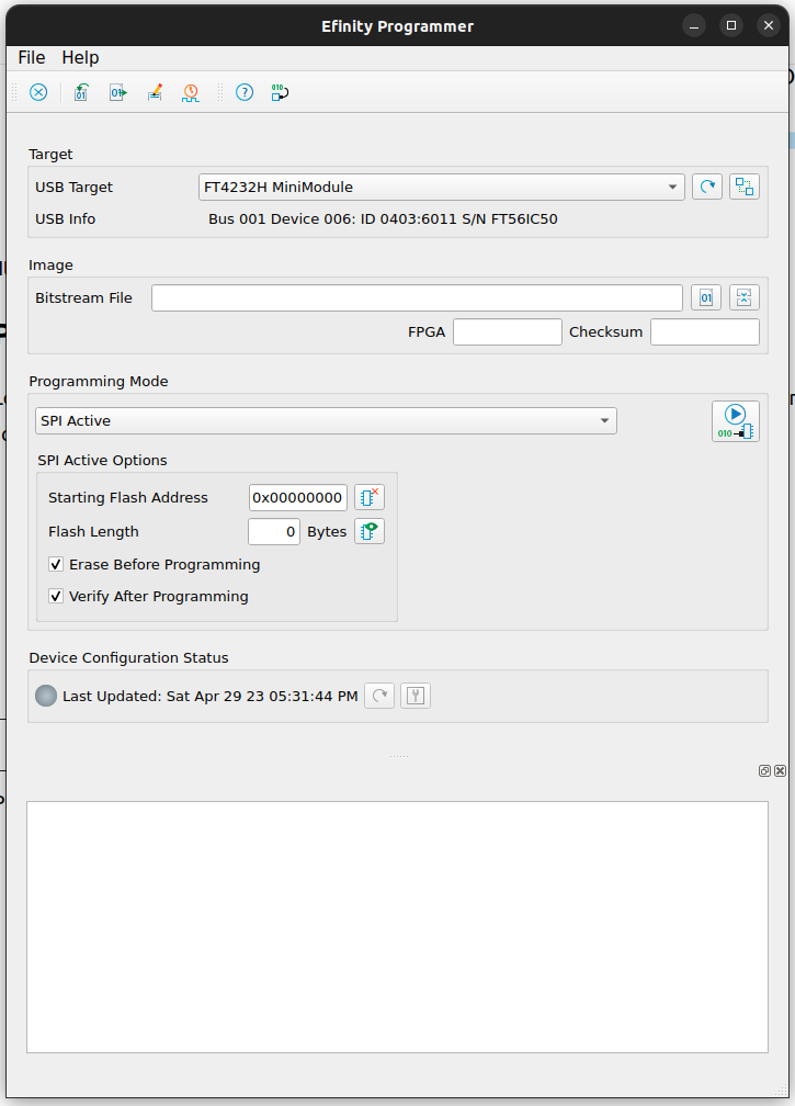
Programming the FPGA through Efinity
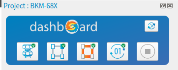
Load the project into efinity and ensure the program is synthesized, routed, etc. by ensuring the flow is “complete” like this:
Efinitys “flow” process
If not, press the (01) button and let it run.
Press Tools -> Open Programmer to get this window:
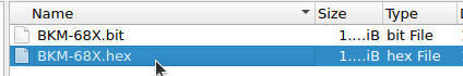
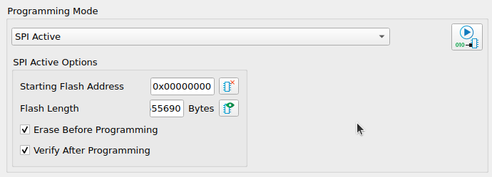
Press the “01” button (“Select Image File”) and select the “.hex” file (inside the outflow directory of the project).
Since I looked into the BKM-15R protocol, I thought it cool to implement it in a small unit, that would give the most minimal required from the controller, meaning input keys, menu navigation and of course power. Enter the BKM-15R-mini.
The BKM-15R-mini
This unit is based on a small PCB with the physical buttons which an ESP32 Devkit V1 board and a ENC28J60 module plugs into. The ESP32 at the same time gives the option of a small WiFi enabled webserver to emulate the “full” BKM-15R.
The “naked” PCBs. The ESP32 module is “raised” by a normal set of 2.54mm/0.100″ pitch female headers. The ENC28J60 is raised further to clear the RJ45 plug.
It might be a good idea to put some insulation between the RJ45 plug and the base board. Either a bunch of kapton tape or something like this.
The base board without the ESP32 and ENC28J60 module.
The board features a kill-switch to disable WiFi if you only want the physical buttons, and don’t trust the air. You can also comment out all WiFi code in the Arduino project 🙂
The first time it is booted up, it looks for WiFi credentials in the persistent storage. If none are found, it goes into a configuration mode, where it creates an access point called “BKM-15R-Setup” and “adminadmin” as the code/PSK (at least at this time of writing, check the code for changes). When connected to this, browse to http://192.168.4.1 where you will see a very rude setup page, to enter SSID and PSK for the WiFi it is meant to connect to. After saving and restarting, if this needs to be changed, press the small “FORCE_SETUP” switch while hitting the “RESET” switch, to force it into configuration mode.
When connected to a WiFi, browse to whatever IP it has been given (you need to check this on your router, or whatever), and you’ll see a representation of the BKM-15R.
The BKM-15R-mini web interface
This is of course not very phone friendly, and might change over time, but here it is…
With the physical keys, you should be able to do most stuff, albeit a bit cumbersome, as setup will need to be done through the menu, but if you utilize the channel stuff of the BVM, it’s pretty powerful.
The ESP32 module can be found quite cheap on the internet, and the same for the ENC28J60 module Note that it should be the “large” version with mounting holes, at least that’s the only version I’ve mechanically tested.
The code for the ESP32 board can be found here: https://github.com/skumlos/bkm-15rduino Note that it is based on Arduino framework (hence the rduino postfix, credit goes to Aaron Bonham for the original idea, as I stole this naming-scheme from his bkm-10rduino project).
This post is still being worked on, but for the sake of sharing, I’ve already made it public so people can start trying some of it. I will update it as I figure out more stuff…
You can find a quick C implementation of this written for the Linux terminal at https://github.com/skumlos/bkm-15r-app
You can also find an implementation for ESP32+ENC28J60 at https://github.com/skumlos/bkm-15rduino
So related to the BKM-68X, an almost just as important unit to have when it comes to the BVM-A series, is the remote control, the BKM-15R. The BKM-15R is a “weird” inbetween unit, switching from the serial RS422 transmission of the BKM-10R remotes, to Ethernet/LAN connections, and apparently “quickly” evolved to the BKM-16R and newer for Sonys professional LCD series. As far as I know, only the BVM-A series use the BKM-15R, and nothing else. While the BKM-16R *should* work for BVM-A monitors, allegedly the function buttons of it do not, which is kinda a bummer, even though you *can* reach most if not all, of that functionality through menus. Still not so cool though. So what to do? Let’s map the BKM-15R and figure out if we can emulate it!
So to analyze network traffic, the infinitely awesome WireShark application comes handy. Since we need to listen in on a LAN connection, the easiest way is to find a managed switch that supports Port Mirroring, so a third unit will get the packets coming in and out of the network ports of either where the monitor is attached to the switch, or where the remote is. By doing this, we don’t interfere with the communication at all, we simply get to see everything going through the interface in question.
The remote has two modes, peer-to-peer and LAN, selected by a switch on the back. Peer-to-peer is when the remote is connected directly to the monitor by a network cable (straight through) and LAN mode is the more esoteric version, where the remote lives on a network with other units. The same goes for the monitor. Everything below relates to remote and monitor being in peer-to-peer mode. While I suspect it should work just as well in LAN mode, I have not tested any of that. Everything here is tested with an original BKM-15R and a BVM-A20F1E.
When the remote starts up in peer-to-peer mode, it first ARP’s “192.168.0.1”. The remotes standard IP address is 192.168.0.100. By default the monitors’ IP is 192.168.0.1. The monitor broadcasts some information about it, like model number and such from time to time.
When the remote gets a positive ARP response, it opens up a TCP socket to the monitor on port 53484.
Packet format
Each packet from remote to monitor starts with a header like this, top part is the “decoded”, bottom raw bytes:
<PAYLOAD_LENGTH> is the length in bytes of the payload. Note that <PAYLOAD_LENGTH> can be zero, and thus there is no data returned.
Payloads
The payloads are ASCII based, meaning everything, even numbers, are encoded in ASCII. Note that the “commands” in the payload are generally separated by 0x20, meaning ASCII space.
Status probing
When the remote has connected, it starts continuously asking for the status of the monitor (roughly every 500ms), and the monitor replies with a 5 word status packet, like this:
Red is the header part, 0x28 is the payload length (0x12 = 40 bytes after the header). Bold parts are the status words. From this it can be seen that the monitors status words are 0x80000x00000x00000x00000x0000.
By pressing the buttons, it can be seen how the status words change depending on what is activated, like if the Aspect Ratio (16:9) button is pressed, the monitor returns:
So the status words are now 0x80020x00000x00000x00000x0000. Thus it can be seen that, just like on the BKM-10R, the status bits are OR’ed together. By going through all the buttons I have deduced the following status bits:
Status word 0:
0x8000 - Power On (CRT On)
0x0400 - Scanmode (Underscan)
0x0200 - Horizontal Delay
0x0100 - Vertical Delay
0x0080 - Monochrome
0x0040 - Char mute (Char Off)
0x0020 - Marker Mode
0x0010 - External Sync
0x0008 - Aperture On
0x0004 - Chroma Up
0x0002 - Aspect Ratio (16:9)

Status word 1:
Unknown / unused

Status word 2:
0x0100 + 0x0080 - Menu is showing (both seem to be on)
0x0040 - Color Temp
0x0020 - Comb
0x0010 - Blue Only
0x0004 - R Cutoff
0x0002 - G Cutoff
0x0001 - B Cutoff

Status word 3:
0x0080 - Phase Manual
0x0040 - Chroma Manual
0x0020 - Brightness Manual
0x0010 - Contrast Manual

Status word 4:
Unknown / unused
Status changing
When a button is pressed, the monitor issues a status change ‘STATset’ packet plus the button name plus the word ‘TOGGLE’ (except for degauss) with spaces between each “part”. So for instance aspect ratio toggle sends:
So by pressing all the buttons, the list of possible status button names are (most quite self explanatory):
"POWER" - Power
"DEGAUSS" - Degauss
"SCANMODE" - Scanmode (Underscan)
"HDELAY" - Horizontal delay
"VDELAY" - Vertical delay
"MONOCHR" - Monochrome
"APERTURE" - Aperture
"COMB" - Comb
"CHARMUTE" - Char Off
"COLADJ" - Color Temp.
"ASPECT" - Aspect ratio (16:9)
"EXTSYNC" - External sync
"BLUEONLY" - Blue only
"RCUTOFF" - R Cutoff
"GCUTOFF" - G Cutoff
"BCUTOFF" - B Cutoff
"MARKER" - Marker mode
"CHROMAUP" - Chroma up

"MANPHASE" - Manual phase
"MANCHR" - Manual chroma
"MANBRT" - Manual brightness
"MANCONT" - Manual contrast
Navigation/input
The navigation buttons and input keypad are split into another “group” of buttons, the INFO group. Presses are announced <HEADER> 'INFObutton' 0x20 <BUTTON_NAME> 0x20. So for instance button ‘1’ is announced like this:
Note the second last byte, 0x31, which is ASCII for ‘1’. Button 2 is then the same packet, except for the second last 0x31 byte instead being 0x32, so (difference marked in blue):
Button 3 is 0x33, and so on for 0-9. The remaining button names are:
"ENTER" - Ent at numeric keys
"DELETE" - Del at numeric keys
"MENU" - Menu
"MENUENT" - Menu Enter
"MENUUP" - Up
"MENUDOWN" - Down
So for example 'INFObutton' 0x20 'ENTER' 0x20 when pressing “Ent” at the numeric keys.
Knobs
The knobs are also part of the INFO group. When a knob is turning, the remote sends a packet about every 150 ms with the string “INFOknob”, name of the knob, and a designation of how far it has turned. An example turning the Chroma knob slowly clockwise:
I am still somewhat unsure of how to interpret the output, except that the 96 is static, the next part (1) can be small or “large” (like 7), usually depending on how fast one turns the knob, positive values are clockwise, negative values counterclockwise. The last part (25) seems to be saying something about how far it has rotated, but I have seen both values be negative, which makes not so much sense.
Here is an example of the brightness knob turning counterclockwise at about the same pace as above:
All in all its a pretty simple protocol that can be reproduced in almost any “normal” programming language and on any platform that supports raw TCP sockets on a LAN connection.
Any questions, comments or whatever, send me an email at martin@hejnfelt.com
UPDATE Read the last part about the 3.3V vs. 5V of the MN5814!
A guy on Facebook asked if it was possible to region mod a NTSC PSone with the original PSone screen attached, to be able to play PAL games also, to which I replied that as far as I knew, the screen is “region” locked, so PAL signals will give a rolling image, exactly like if your VHOLD on a CRT is “out of sync”. I remembered I had a banged up SCPH-130 monitor, which as far as I know is the first Japanese revision (unsure tho), and is thus NTSC, so I tried it out on my modchipped and DFO’ed EU/PAL PSone (SCPH-101), and true enough, when playing PAL games the picture would begin rolling.
Chipped PSone playing a PAL game (Die Hard Trilogy) on a NTSC SCPH-130 TFT screen.
Since the screen was already pretty banged up (not my doing) I decided to investigate and see if I could determine *what* was actually causing this.
It should be noted that there are several revisions out of this monitor, and I have no idea how other revisions work, so your mileage may vary.
Anyways, to disassemble the monitor, you need to remove the speaker grille, at least in the outer corners, as there are two screws in each side here. Note that I would assume it quite easy to destroy the grille (and end up with a result like mine), so take care.
When all screws are removed you should be able to pry the back cover off, and see the main PCB of the monitor:
The SCPH-130 mainboard.
So there are three large IC’s which is of interest here. IC12 in the middle which is an AN2526NFH signal processor (“jungle” IC), IC1 in the bottom which is a MN5814 “TFT AV Panel Controller IC” and IC3 which is a Wiseview LTS5QTB. The latter I couldn’t find any information about, but since it isn’t important, who cares.
So looking at IC12 it has a ~3.57MHz crystal, the color carrier frequency for NTSC composite signals, and thus is wired for NTSC. Looking at the datasheet, the unit does support PAL (with a 4.43MHz crystal instead, and another color trap filter), but since the PSone is connected via RGB, PAL/NTSC shouldn’t matter.
The MN5814 is apparently a controller for TFT panels, so I looked at the datasheet to see what its pins did. Here I noticed the NP1 (pin 46) which is labeled “NTSC/PAL” in the pin overview. This pin has a built in 100K pull-down resistor, and whaddaya know, there’s a test pad labeled NP1 on the SCPH-130 mainboard!
The MN5814 TFT controller. Notice the NP1 pad in the top left of the IC.
The datasheet I had didn’t mention much about what level did what, but measuring it out, it is pulled low by the internal resistor. I thought that I’d try to pull this high, so I did that, and voila, now NTSC was rolling and PAL video was steady! So to “fix” the issue, this pin needs to be toggled depending on the video type.
I tried looking around for a suitable signal, but couldn’t find any, but I found a bunch of VSYNC pads, including one called VOUT at the AN2526NFH.
AN2526NFH. Notice the pads to the right top of the chip.
There are 4 pads, bottom is labeled FIELD, next is VOUT, then HOUT and then BURST (VOUT, HOUT and BURST labels are further to the right just after the caps).
I took a scope and measured VOUT, and could read that it was the discrete VSYNC output. To prove that my hypothesis worked, I took an Arduino Nano, wrote a very small program that measured the VSYNC duration, and from that decides if the VSYNC is 50Hz or 60Hz. I do this by connecting VOUT to INT0/D2 (interrupt 0) so the MCU runs a piece of code when the signal changes state, and then measure the number of milliseconds from LOW to LOW (using millis() function). Above 18ms I decide it to be 50Hz (which is ideally 20ms) and below is 60Hz (essentially ~16,7ms). Below 12ms is considered “noise”. Applying the decision to an output and then connect that output to the NP1, and *pling* everything now works! You can find the code here: https://github.com/skumlos/frqdetector
The same setup as previously, now with the Arduino attached.
Now this is very crude, I don’t even know where to put the Arduino, but maybe using a Mini Pro or any smaller footprint Arduino compatible board, or writing a version that works for the PIC12F508 which is really common for modchips, I suppose that would be much better (or any ATTiny or whatever).
The Arduino is powered by the 7.5V point in the bottom of the PCB near the hinge and whatever GND point.
The NP1 pad connection.
The VOUT pad connection.
The Arduino Nano (notice the 7.5V pad in the top right)
UPDATE It was brought to my attention that the MN5814 is running on 3.3V and not 5V. Since the Arduino is (usually) running on 5V, it’s I/Os are also 5V. The MN5814 specifies that max. I/O voltage is VDD+0.3V (meaning there’s most likely a diode there) so it is advisable to run the NP0 output from the Arduino through a voltage divider, like two 1K resistors, and then pull the NP0 signal between the two.
Fun stuff! Any ideas or something for this? Let me know! martin@hejnfelt.com or skumlos/skum on various boards.
So I bought a Sony BVM-D9H1E to be able to test my BKM-129X boards at 31kHz (480p) and above. Being a *1 unit and not a *5 (like D9H5E) it has no integrated controls, and thus need an external controller. This can be either a *5 unit, a BKM-10R, or in this case the BKM-11R which connects to the front mini-DIN 8-pin option plug.
BKM-11R remote controller
The 8-pin mini DIN “OPTION” plug of the D9H1E.
Now the controller has a DE-9 port (and another mini-DIN 8-pin plug to daisy chain further to units like the BKM-14R probe) which therefore requires an adapter cable to the mini-DIN.
The DE-9 port to the right that connects to the monitor, and the 8-pin mini-DIN to the left.
The cable didn’t come with my remote, so I needed to make a new one. Searching the internet brought me to the shmups forum where this picture exists:
The top picture is the DE-9 port of the BKM-10R and the bottom is the mini-DIN. Unfortunately the BKM-11R does *not* use the same pinout as the BKM-10R seemingly, because making a cable from the above doesn’t work. I opened up the remote and could see that ground and 5V were definitely not the same, so I started searching for answers. Although 5V and GND are easy to measure out, the TX/RX pairs are not so easy as they’re seemingly buffered by the remote for the mini-DIN port.
I was unable to find a service manual documenting the the remote, so I was kinda lost. The next step was of course to disassemble the remote further to see if I could decipher further, but then awesome guy Steve Nutter of Retro Tech (he does a lot of informative CRT related videos on YouTube, check it out if you don’t know him https://www.youtube.com/channel/UCwOTvOtoAjiqQx1PCrfmTKw) measured a working cable out, which then made it easy to make a replacement. The pinout is as follows (pin numbers are as a normal DE-9 plug): 1 – NC 2 – RXD 3 – TXD 4 – NC 5 – GND 6 – 5V 7 – ~TXD 8 – ~RXD 9 – NC
Thus to make a cable, using this pinout, along with the information fromt the shmups post by xga, the connection needs to be like this:
Signal
mini-DIN (monitor)
DE-9 (controller)
TXD
8
3
5V
7
6
RXD
6
2
~TXD
5
7
GND
4
5
~RXD
3
8
Mini-DIN female pinout (taken from Schurter 4850.2810 datasheet)
For cable, I simply used an normal unshielded Cat5E ethernet cable, and then use a twisted pair for TXD/~TXD and other pair for RXD/~RXD.
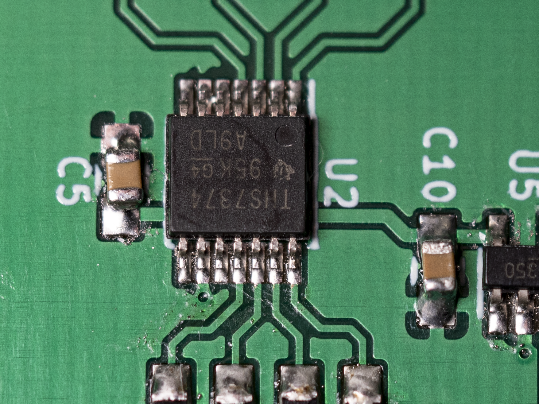
So I’ve found out I’ve made a huge mistake on my BKM-129X designs (all of them): The low pass filter of the THS7374 is *not* disabled as was intended. As I myself have no hardware to test 480p and above, so I never noticed the issue, but Bob from RetroRGB.com noticed when running 720p sources through it, there is a softness to the picture which shouldn’t be there. This is because I erroneously connected the BYPASS pin of the THS7374 to GND instead of VCC. This means that instead of disabling it, it is enforced. Nobody likes this filter, and it should never have been enabled! For 240p/480i/480p the filter makes no difference so if this is what you’re using the board for, don’t bother, but for 720p/1080i it makes a huge difference. Luckily the fix is rather easy, and can be carried out on already assembled boards.
Disconnecting BYPASS from GND
First thing to do is get the BYPASS pin (pin 9 of U2) disconnected from the GND plane.
The THS7374 (U2) chip. BYPASS/Pin 9 is the bottom second pin from the left, right above the via (the black dot). Picture courtesy of RetroRGB.com
Pin 9 is connected to the GND plane through a small trace right in front of it. We need to cut this trace (or lift the pin). I prefer cutting the trace.
This small trace marked with red should be cut/removed.
Use a scalpel or boxcutter blade to gently cut it. Its not very thick but its important to ensure the connection is completely gone, and at the same time ensure the via is not destroyed. The pin to the farthest left is not connected to anything, the other is VCC. Measure that connection to GND is gone by using a multimeter set to measure resistance.
Connecting BYPASS to VCC
After severing the pin, we need to connect it to VCC to force the low pass filter off. Luckily the pin right next to it, to the right, is VCC. The easiest is simply adding a small blob of solder to the two pins.
The BYPASS pin bridged to VCC pin (pin 10).
That’s it. Enjoy 720p, and sorry for the inconvenience.
– or “How my love for logic analyzers is re-affirmed”
This is both a documentation project as much as a reference for myself. I will update this as I figure stuff out, so this article is in no way “final” (yet). I’ve decided to release it as openly as possible, mostly to maybe get feedback and ideas, but also to show the world that reverse engineering projects of the BKM-68X *is* being done. Please send me any ideas or thoughts about the project (martin@hejnfelt.com) but please no “When is it done?” and alike. It might come “soon”, it might come never.
In the current world of CRT enthusiasts working with professional monitors, there are few input cards that has a more elusive status than Sony’s BKM-68X, the analog RGB/YPbPr input card for Sony’s BVM-A series. This card is the only way to get analog component signals into the BVM-A series, at least without any converters. The BVM-A series came very late in the CRT era, and thus lot of production had already shifted to digital formats and utilized digital formats like (HD)SDI as the transport, instead of analog formats. This seemingly means that there are very few BKM-68X in existence (the talks are around 1000 units) in comparison to the number of available BVM-A’s, which then usually sports the (HD)SDI card BKM-62HS and maybe the BKM-61D (SDI and composite/S-Video). The scarcity of the BKM-68X means that they often sell for more than $2000 a piece, if they are even available. Given that the A-series are young monitors, they are desirable given that their tube-time is often quite low.
So, in the world of retro-gaming, digital formats, especially not SDI are usually not desired, while young tubes, high TVL and RGB is are. Shelling out $2000+ for a input card is however insane for many, which often leaves BVM-A monitors undesired (there are some other issues with the 68X/BVM-A, especially sync wise, but forget about that for now). In general increasing the availability and decreasing the costs of the BKM-68X, would be helpful for the retro-gaming community, which makes it a good candidate for reverse-engineering.
When I released the reverse engineered BKM-129X card, a lot of people asked me about the BKM-68X, to which I normally replied “Forget it”. This was because the design is *massive*. The card has so many components that it looks like the surface of the Death Star, and if some X-Wings appeared trying to find an exhaust pipe to bomb, nobody would really find it weird. At the component level, Sony has also blessed us with black-box units like a FPGA plus a CPLD at the same time, so yay!
The BKM-68X. Picture is courtesy of RetroRGB.com.The Lattice CPLD and Xilinx Spartan FPGA. Picture is courtesy of RetroRGB.com,
One night however, my life was apparently going so slow, that I ended up looking at the service manual for the card (most likely to avoid watching Dora the Explorer, Bob the Builder or alike), which sports the full block diagram and schematics to the card. By looking at the signal names for what is seemingly thrown around on the IO connectors (of which there are two 100-pins) and by looking at the signal paths, it made me believe that the card is seriously over-engineered, at least in the context of retro gaming, and that many features can be simply omitted, if the goal is not a replica but a basic “alternative” which supplies RGB/YPbPr to the A-series, and that’s it. It’s my belief that this would be beneficial to 95% of the A-series owners, of which I suspect very few are professional video editors, and many retro-gaming enthusiasts.
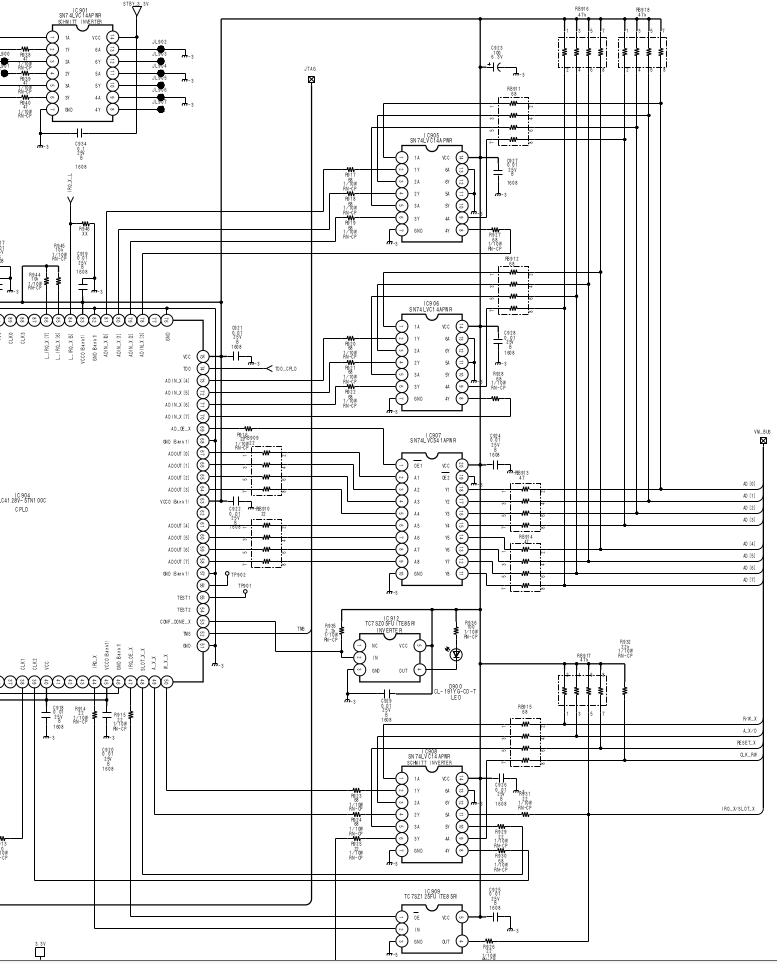
What really made me interested was this part of the block diagram:
The block diagram for the interface between the BKM-68X’s CPLD and the monitor.
Plus the part of the video signals:
The video signal portions of the BKM-68X card.
Now the CPLD interface suggests a quite standard parallel interface of a shared address/data bus, plus the video signals seemingly are normal analog RGB/YPbPr along with separate horizontal and vertical sync signals.
All around the board are signals which are generally in the same “vicinity” to the ones of the BKM-129X, namely: VIDEO_OE_X (video output enable, active low), INT/EXT_X (internal/external sync, active low), HD/SD_X (high definition/standard, active low) and so on. There is some circuitry that seemingly seems able to do some “magic” to the input, like an aperture generator (I have no idea what that should be doing) but in the end, I this seems to be non-vital. In general though, looking at the signal paths for the RGB signal paths, they basically do through some filtering and buffering, with some different paths (filtering orders, delay lines) selectable by the HD/SD_X signal. It all ends up in the IC486, which is a AD8075ARUZ which is a 500MHz 6dB video buffer, that is still easily obtainable (and should most likely also be replacable by something like the THS7374).
As the address/data bus should be able to be “eavesdropped” on, exactly like the SPI-like bus for the BKM-129X, it is my firm belief, that a viable alternative can be created.
Of course reading the contents of the EEPROM for at least the FPGA could be possible, but using the data would be against the law in many countries, and in the end also still require the same FPGA unless the bitstream was then reverse-engineered.
Accessing the hardware
To be able to actually do such a project, the original hardware is strictly necessary. Fortunately I was gifted a BVM-A20F1M with a BKM-15R for the project. The BVM didn’t have the BKM-68X, but it did have the BKM-62HS, so it was a start, even because the 62HS’s digital signals still end up as analog video coming into the monitor. Technically, this would mean that even just ending up being able to impersonate a 62HS might give a “workaround” card. However seemingly the card supplies YPbPr to the monitor, plus there are some horizontal scan rate “issues”. Jumping a bit in time, I was lucky to get an original BKM-68X donated to the project, which opened up the possibilities to make a board much closer to “what we want”.
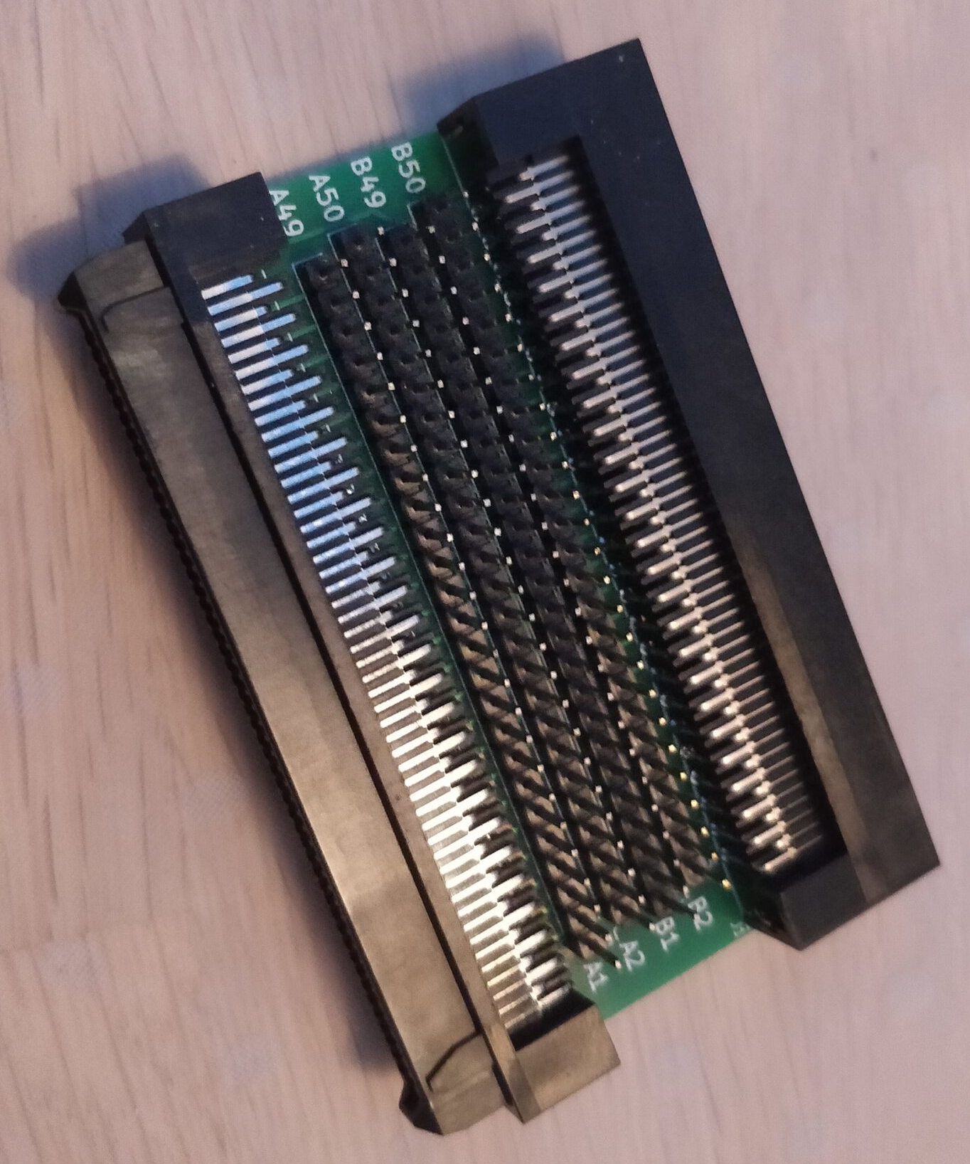
To eavesdrop on the communication, I developed a small “breakout” board that could be inserted between the monitor and the card, which breaks out each 100-pin connector:
BVM-A card breakout.
The connector is a JAE TX24-100R-LT-H1E (mating with TX25-100P-LT-H1E). This card allows me to easily attach the probes of my logic analyzer and listen in on how the card and monitor speaks to each other, exactly how I also dealt with the BKM-129X card. I still need to solder a couple of wires onto miscellaneous spots of the board, as to find the command sequences for the different “options” (internal/external sync, RGB/YPbPr etc.). This is kinda fear inducing when you start to solder onto a $2000+ card. Luckily though, there are some resistors at all points of interest that can be used:
Also to be sure how the data exchange works I needed to figure out when the data bus is driven by the CPLD and when it is driven by the monitor. As can be seen in the service manual, the CPLD has 8 address/data (A/D) lines in and 8 A/D lines out, both “buffered”, but the A/D out lines, has an “output enable” signal (AD_OE_X) attached to it. The same goes for the IRQ_X signal which is tied to the IRQ_X/SLOT_X signal, through a buffer, which is enabled by IRQ_OE_X signal. These signals can be observed at:
IRQ_X @ R914 IRQ_OE_X @ R915 AD_OE_X @ R916
The address/data bus and relevant control signals.
The signals of interest are thus:
AD[0:7] (8 bits/1 byte) – The address or data byte being transmitted A_X/D – A/D byte is address when this is low, or data when it is high R/W_X – Data is read when this is high or written when low CLK_RW – Data is latched on the this, seemingly on positive edge AD_OE_X – Address/data bus is controlled by CPLD when this is low IRQ_X/SLOT_X – Seemingly when this is low, the monitor interrupts the card *OR* when IRQ_OE_X and IRQ_X is low, the card interrupts the monitor RESET_X – Reset the card on low
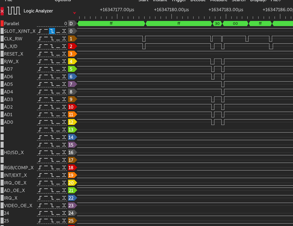
So 15 signals, plus the 4 internal-card signals (VIDEO_OE_X etc.) meaning 19 signals. To do all this at once, I had to upgrade my logic analyzer to more channels, so I bought one of DreamSourceLabs DSLogic U3Pro32 and srsly, it’s awesome. If you need a cross platform logic analyzer, I can recommend this (I use Ubuntu/Linux as my primary OS).
As with the BVM-D9 and D14, the monitor starts speaking with the card already at standby-power (when the mains-switch on the back of the monitor is flicked), so I set the logic analyzer to sample at 20 MHz for 50 seconds from when I flicked the switch, and ho-lee-phuck, these monitors speak, jesus christ.
Analyzing the data
So here’s a screenshot of DSView of the data:
Initialization, settings are RGB with External sync (no signal input)
So first, again, there’s a lot of data, and at first, I noticed that CLK_RW pulses were 50 ns (20 MHz) in width, which means when I sample at 20 MHz, I’m not upholding Nyquists Sampling Theorem, which says that to properly sample something at frequency X, you need to sample at 2*X. This means that I needed to redo my measurements at 50 MHz (next available sample speed on my analyzer) at least if I wanted accuracy in the timing between edges. Doing this showed that clock pulse widths are 40 ns so 25 MHz(!). At first I was unsure of what to make of all this data, because according to the service manual of the monitor, each slot has a separate SLOT_X_INT_X signal *and* CLK_RW signal. This would indicate that it would only clock data to the card (with CLK_RW signal) when it was speaking to the specific card. Seemingly all these data points are clocked in, which would, at first glance, mean that all this data was bound for the card. Luckily after “working” through the data, I got an “epiphany”: The card “changes” which commands it reacts to depending on which slot it is in, and this is actually somewhat of a kicker, because it narrows the amount of data to react to considerably down. The idea can be seen here:
One of the first command sequences, here card is in OPT1, so first slot.Same sequence, but a “block” later, when card is in OPT2, so second slot.
So first the monitor issues a 02h command, followed by 01h which asserts IRQ_OE_X (interrupt output enable, active low). Then comes FFh (which denotes a start and end of command sequences, as will be seen later). Then it issues a of 10h03hXX (XX = 01h-07h), FFh then 02h 00h which de-asserts IRQ_OE_X again (thus seemingly allowing interrupts from the card again). Now in the first picture, it can be seen that SLOT_X_INT_X goes low in the 10h 03h 02h (where the card is in OPT1 slot), but in the second picture, it goes low during 10h 03h 03h (where the card is placed in OPT2, so the second slot). As the first slot is actually the network card (or whatever we call it), where the remote and such is placed, it makes sense that OPT1 is actually slot 2 (in the monitors sense), OPT2 is slot 3, OPT3 is then slot 4, then comes whatever the other “cards” are in 5 and so forth.
EDIT: Using my eyes, the monitor even says so 😀
The monitors label explaining the slots.
When the card is in OPT1 as the only one, it reacts to commands in the 2Xh, while in OPT2, it reacts to 3Xh. The monitor does try to read 3Xh and 4Xh addresses, from time to time, but when there is no card there, nothing responds.
Blank read from 30h 00h when card is in OPT1.Blank read from 20h 00h when card is in OPT2. Succesful read from 20h 00h (returning 88h) when card is in OPT1.
So all in all, we can now assume that only commands starting with 2Xh is actually intended for the card, when sifting through the data recorded when the card was in OPT1. I will generally show 2Xh commands as I’ve got most data from the card in the first slot, so in all those cases, practically the first byte could be 3Xh or 4Xh if the card was in OPT2 or OPT3 respectively.
Command format
From this it can be deduced that the general command format is like this:
First the monitor issues a FFh with AX_D low and R_WX high. Then it writes a “command/register byte”, then an “offset” byte, and then the actual value (either read from, or written to, denoted by R_WX), and then a FFh more.
So an example as above is FFh 20h 00h 88h FFh, where R_WX is high on the last byte, meaning the monitor is reading byte 00h from register 20h, in the above example, this returns 88h.
For the two “special” commands, 02h (IRQ) and 10h (setup/init) it starts with the command, and ends with FFh.
Here is an example of a write:
A write sequence
So here it writes A0h to 32h 25h, so FFh 32h 25h A0h FFh.
Card identification
So first part is figuring out where the card is actually being identified. Analyzing the data from the BKM-68X, BKM-61D and the BKM-62HS shows that the first difference lies in the response of the read from 20h 00h, which responds 88h on BKM-68X, 81h on the BKM-61D and 82h on BKM-62HS. This also the first command issued to the card, before all the serial stuff and whatnot begins.
Serial number readout
Command 23h seems to read the serial. The serial must be read out from some PROM by the card internally somewhere, as I suspect the Xilinx FPGA actually contains a softcore CPU or something, because there are some “wait-states” where the monitor issues some command, then repeatedly reads some register until it turns to some value (00h), then reads another register, seemingly verifying its contents, and then repeats the process if not “accepted”. One of those registers is the serial, first byte, 23h 00h. Initially the monitor issues some commands, reads a register until it turns 00h, then reads 23h 00h, which returns 88h (like the identification register). If this is the case, the monitor re-issues the command sequence, reads the register, repeats until this register returns at least 32h, which is the first byte of the serial (just as with the BKM-129X, this is ASCII coded digits, so 32h is 2). The complete serial is then located in registers 23h 01h, 23h 02h etc. until 23h 06h as there are 7 bytes in the serial (eg. “2 0 0 1 3 3 7” would be represented by 32h 30h 30h 31h 33h 33h 37h), so: 23h 00h 32h 23h 01h 30h 23h 02h 30h 23h 03h 31h 23h 04h 33h 23h 05h 33h 23h 06h 37h
Video format settings
Command 21h seems to work on the video settings.
Register 10h (21h10h) works on (at least) VIDEO_OE_X (video output enable, active low), INT_EXT_X (internal/external sync, low = external) and APA_ON (Aperture). The bits of the data byte I’ve identified are: Bit 3 is VIDEO_OE_X (0 = VIDEO_OE_X -> HIGH, 1 = VIDEO_OE_X -> LOW). Bit 2 is aperture (1 = APA_ON -> HIGH, 0 = APA_OFF -> LOW) Bit 0 is INT_EXT_X (1 = INT_EXT_X -> HIGH, 0 = INT_EXT_X -> LOW).
Register 31h (21h 31h) is the detected video format. This detection is seemingly done by the card itself. When the card detects video, it de-asserts the SLOT_X_INT_X signal, thus interrupting the monitor, which then issues some commands, including reading this register. I’ve identified the following data byte meanings (21h 31h XXh):
00h – No video input 01h – 576i / 50 Hz (verified with EU Wii/EU PS3) 02h – 480i / 60 Hz (verified with US SNES) 03h – 576p / 50Hz (verified with EU PS3) 04h – 480p / 60 Hz (verified with EU Wii) 0Ch – 1080i / 60Hz (verified with EU PS3) 12h – 720p / 50 Hz (verified with EU Xbox 360) 13h – 720p / 60 Hz (verified with EU PS3)
I need further units to know the values for other supported, however my guess is that some of the others are: 0Bh 1080i / 50 Hz
1035i/60 and 1080i/48 I have no idea about…
Given the supported formats here:
Supported formats from the BVM-A20F1M manual
So when the card detects an input (change) it de-asserts INT_X (which de-asserts SLOT_X_INT_X), and waits for the monitor to issue a sequence of commands.
Impersonating the BKM-68X
So to make a “clone”, there are some hardware requirements we need to meet, which does go out-of-spec compared to normal microcontroller options, namely the 25MHz I/O capability. Given that the 68X *and* the A-series are pumped full of FPGA and CPLD technology, the obvious choice is to use a FPGA.
Fast forward some time, I’ll fill in the blanks at some point (everything will be open sourced), it works!
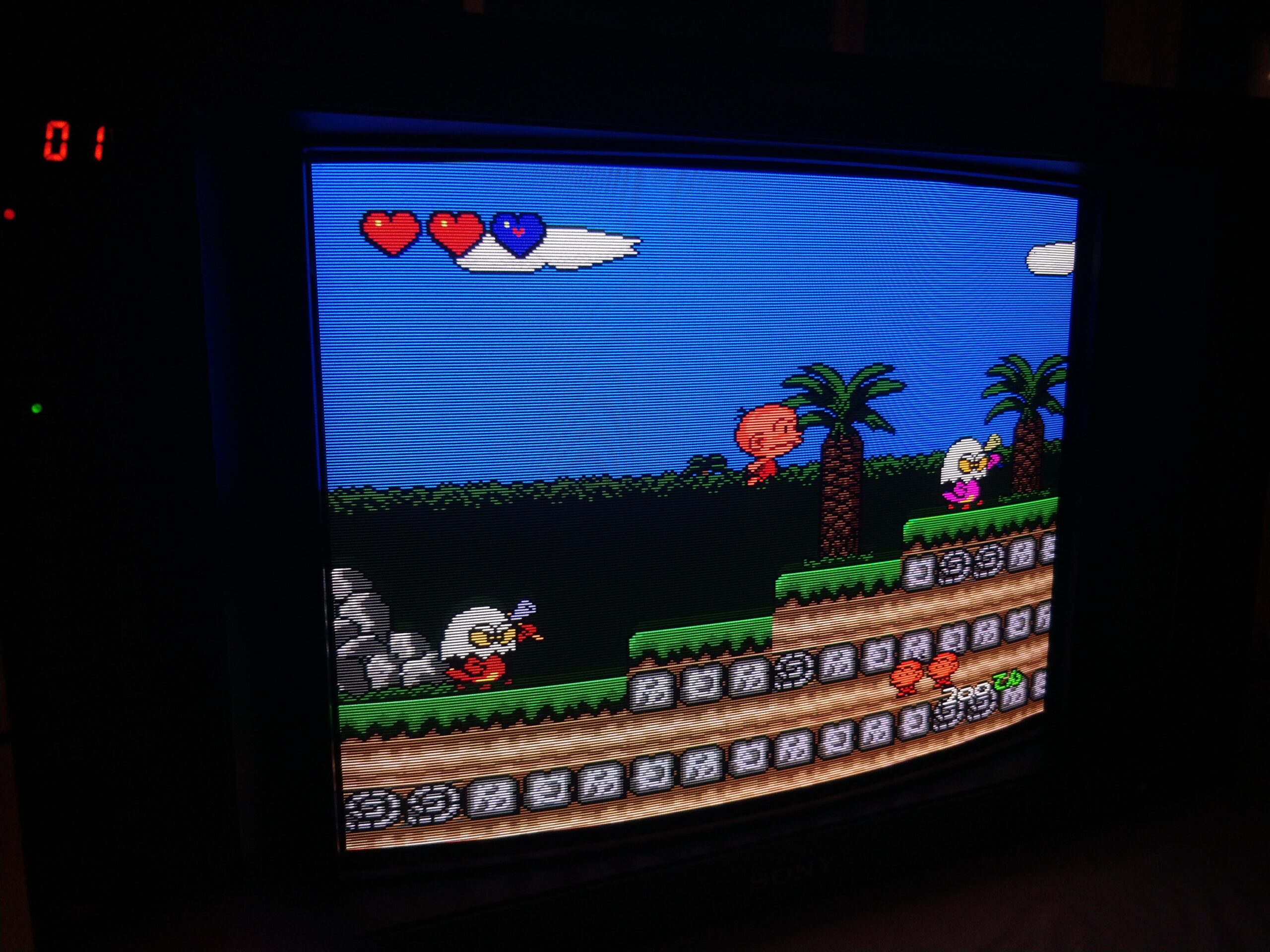
The BKM-68X “clone” showing 50Hz/PAL SMS (60Hz/NTSC works also)Here showing PC engine (white original, with my external RGB add-on)
This should also work for PVM-9L1, PVM-14L1, SSM-20L1 (confirmed) and in the end also other monitors using TDA9394H jungle, at least if you can get to the service menu. Note that capacitor numbers will be different for others. Check the service manuals and verify according to the jungle pins.
So a guy approached me because he had a PVM-20L1 without RGB, and asked if it was possible to mod it for RGB SCART. The unit uses a TDA9394H jungle which is very sparsely documented on the web. There are some mentions of it on the RGB mod thread on shmups and some different documents at least showing the pinout. These pinouts show that it has a separate RGB/YUV input on pin 50 (INSSW2/blanking), 51 (R2/Y), 52 (G2/U), 53 (B2/V), so that is our point of interest. Now the jungle is one of Philips’ which are known to have bits to disable/enable these kinds of inputs through I2C, usually the bit is called IE1 or IE2 (for Interrupt Enable), and this is no exception.
Enabling RGB
Looking in the service manual for the PVM-20L1 there is a walkthrough of the service menu, where the IE2 bit is shown/mentioned, and that relates to this external input. Thus we need to enable this bit.
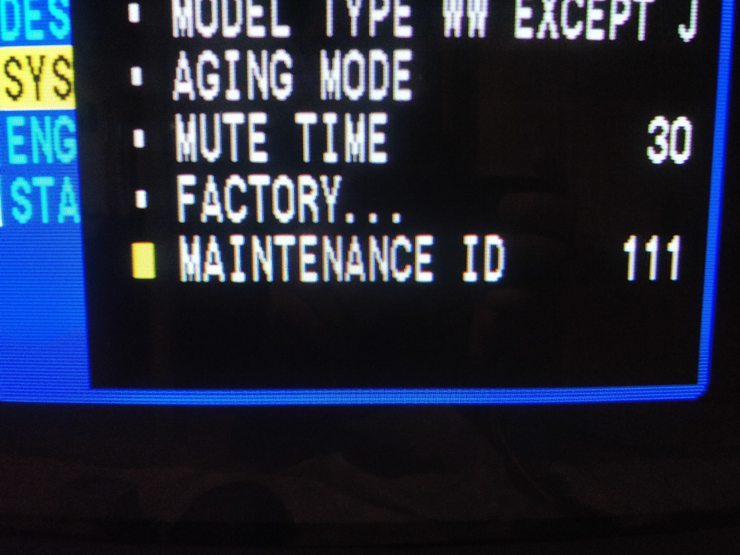
TLDR; Open the service menu (Menu then Menu+Enter for 5 sec), SYS->Maintenance ID=111, DES->CONTROL0->IE2=1, ENG->Comb filter=Forced, save by Menu+Enter for 5 sec.
The service menu is accessed by pressing Menu once (so the “normal” menu comes up) and then pressing Menu and Enter simultaneously for 5 seconds.
The service menu.
Using + and – keys and “Enter” (“Menu” goes back), go to SYS and change Maintenance ID to “111”, press “Enter” to accept.
“System” menuSetting “Maintenance ID” to “111” unlocks the settings we want to change.
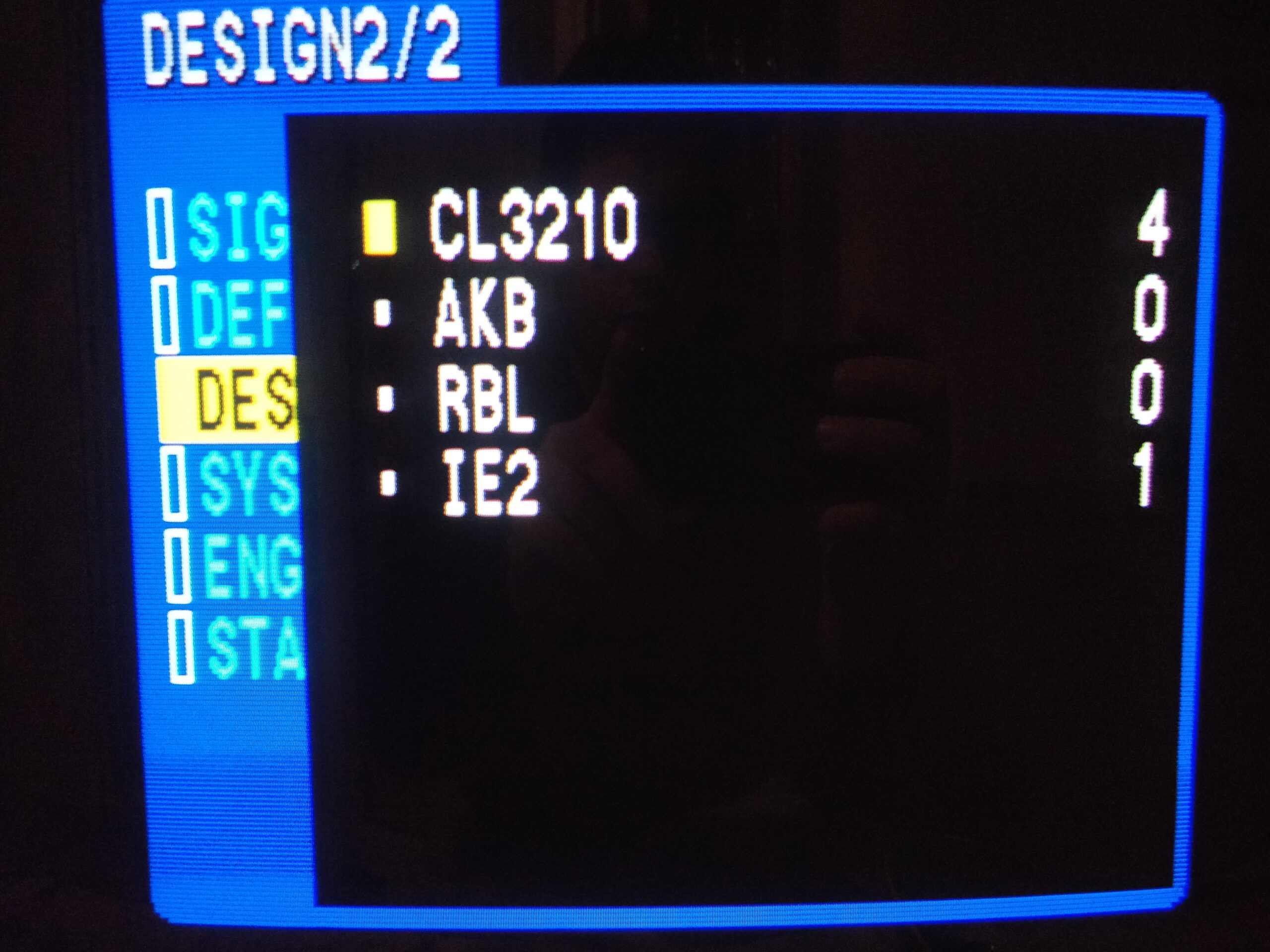
Then go to DES (Design) and into CONTROL0 (on “page 2”). Here the IE2 bit is found so set it to 1. Press “Enter” to accept the setting.
Enable IE2 bit.
Right now, if we had everything hooked up, we’d see a nice RGB signal, BUT IT WOULD BE IN BLACK AND WHITE!!!1
So after going nuts about this, I talked to MarkOZLAD whom many might know from shmups and the RGB mod scene in general, and he hinted that he’d heard that the TDA93xx units needed CVBS for sync to have colors… Aha, so I tried this, and whaddyaknow, it worked.
Ok, but I have CSYNC cables for many consoles, so the suggestion was to create a board that encoded RGBS to CVBS and use that as sync source, to be able to support all RGBS inputs. This can be done “pretty” by using an RGB amplifier like THS7374 along with an AD724/725 RGB to CVBS encoder, and then feed the CVBS to sync, and RGBS to the TDA9394H. I actually begun a board for that, until I stumbled upon some people discussing the same jungle on the CRT Discord. Here a guy, “nut” had apparently fixed this (on a similar PVM I think) by changing “Comb filter” setting from “Auto” to “Forced”. Now this setting I had not seen, and I had been through them all (I thought) so I went back to the service manual, and goddamn, it was there, but NOT under the DES, but instead under ENG (and still needs “Maintenance ID” set to “111”). Flipping that, and glorious color was back! Thanks Mr. “nut”!
The “Comb filter” option
Now the “Comb filter” option is apparently since software 1.2, I don’t know what it looks like on earlier.
Hooking up RGB
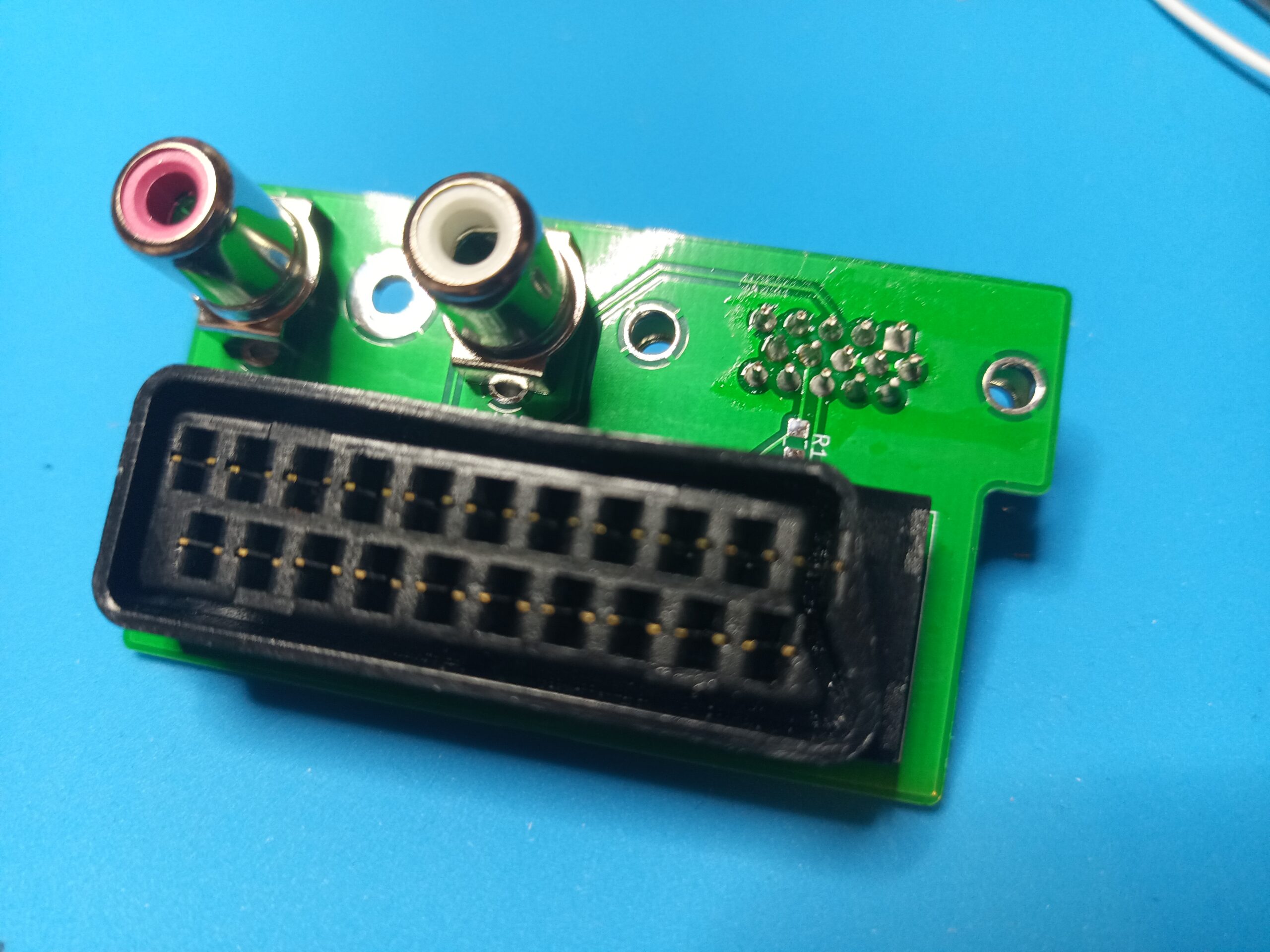
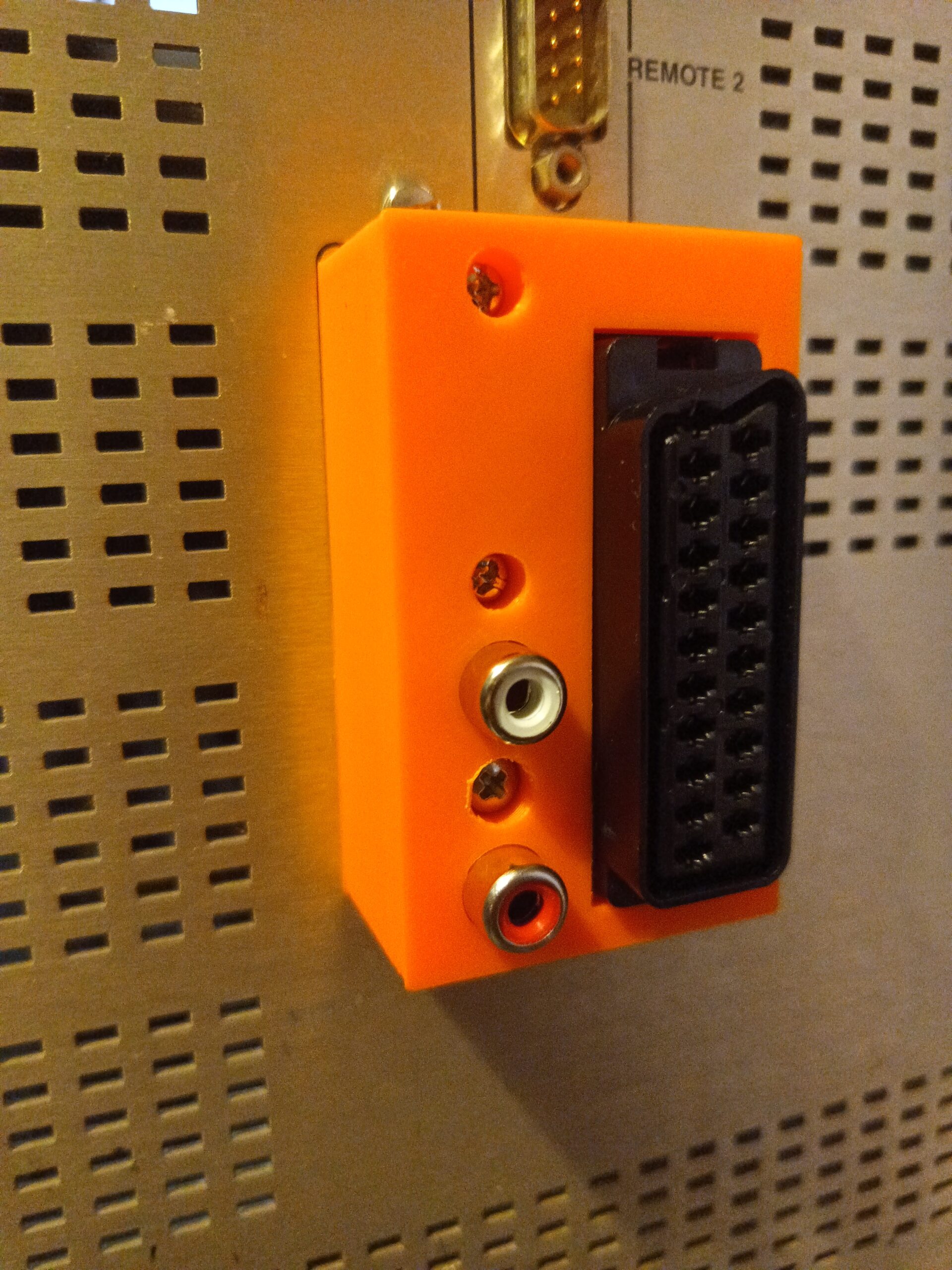
So now to actually hooking up the wires. I will be using the SCART board which I’ve used several times, and I will be injecting each 0.7Vpp RGB signal directly through a 0.1uF capacitor, after 75 Ohm terminating them. The SCART board can be found here: https://oshpark.com/shared_projects/JpxJNG1c
The TDA9394H is situated underneath the main board, so in order to get to it, you need to more or less remove it from the monitor. Pull off the metal case and plastic back, by removing the screws. Pull it backwards a bit, then up. There are a lot of wires to disconnect, find what works for you best. Tip: The small grounding “clip” which there are two of on the tubes lower left back, has a small “release” that needs to be pushed backwards to remove it.
Remember to discharge everything (there seems to be bleeder resistors, so if you have left it unplugged after some time, seemingly there is no charge, but warning warning)!
The TDA9394H jungle.
So locate the jungle that looks like above, and locate the 4 capacitors, C065, C066, C067 and C068.
The capacitors of interest
We need to remove them all, at least C065/66/67, but I took them all. For future reference changing C068 to a 1K resistor here might make sense, but I placed it elsewhere (and didn’t wanna take it all apart again).
Caps removed
Now injecting can be done on either the cap pad or on the small test/solder pads on the traces. I chose the test pads. Now C065 was blue/B2, C066 was green/G2, C067 was red/R2 and C068 was blanking/INSSW2.
The pads I used. Purple is blanking.Wired up. You also need GND of course. White is blanking.
Now bend the cables onto the other side, from the front, as the sides are not accessible due to the “rails” that the board slides into.
Cables, cables, cables!
Attach the RGB to a circuit like this:
As stated, I have this on the SCART breakout board, but if you use other connectors like BNC, do your thing. Note that when IE2 bit is on, INSSW2 is weakly pulled to 5V. Thus if you need to switch to composite, you should add a 1K resistor between blanking and GND, and switch that, or add the resistor and blank with 5V (I use RGB blanking/pin 16 from SCART).
Add sync directly to the BNC inputs (on the PCB) and the same for mono-mixed audio to RCA input. I used input B.
Yellow is sync, white is audio.
So with that, turn on, select input B, and RGB input on 20L1 and friends is now possible! Then comes the fun of physically putting the SCART or BNCs or whatever somewhere…
Attaching SCART
I use the “normal” SCART breakout I’ve used before. R1-R3 should be 0 Ohm, R6-R8 should be 75 Ohm, C1-C3 should be 0.1uF. R4/R5 and C4 are thus unpopulated and JP1 is bridged as we connect directly to the composite input.
So the back plastic part is attached to the metal casing by some plastic rivets. Now these can be removed by simply putting a flathead screwdriver in and they pop out. It is however not a very durable solution in my experience, and I have no idea how easy it is getting spares, so I spent some time contemplating on how to attach the SCART to the back while still being able to remove the whole thing and not tear everything apart. The solution I came up with was soldering connectors to the SCART PCB thus making the wires detachable from the PCB.
The SCART PCB with connectors on. You can see the small 1K resistor between blanking and GND if you look closely. The split connector is simply because I didn’t have any 10 pin angled ones.
Now as can be seen, I needed to make an opening in the side of my normal SCART bracket and then I designed a small detachable cover for it. To get the wires out, I clipped a little of the grille out. The designs including FreeCAD source can be found here: https://www.thingiverse.com/thing:4726360
The small “lid” for the bracketThe grille clipped out
The finished system then looks like this:
The disconnected wires.…and attached
And of course some pictures
Sonic 4, best SNES game ever.The “That guy with the brown jacket” game!