This is somewhat of a “short” post as I haven’t done the mod myself, but it has been verified that my software also works on this monitor. It’s mainly to index that it is possible to RGB mod it, using the I2C interception method as I’ve described for several other JVC monitors. Pictures and schematics should be credited to Victor Clausson.
The mod is somewhat closer to the DT-V100CG mod than the TM-A140PN one, as the jungle of the TM-H140PN is a TA1276AN and not a TB1226EN as the TM-A140PN uses. This means the software for the Arduino to be used, should be this: https://github.com/skumlos/ta1276an-i2c-bridge
Update regarding the Arduino software
Some time ago, an user told me he had a problem with the RGB dropping out every 4-5 seconds, being worse with some consoles, and others showed rare dropouts. We never solved it at the time. Another user contacted me with the same problem recently and we seemingly successfully fixed the issue, and version 1.2 of the software was made. If you’ve already done this mod with 1.1 of the software, and experience this issue, try upgrading to version 1.2.
Now just as with the other mods, the jungle needs to be isolated, and the Arduino put in-between the monitors microcontroller and the jungle (refer to some of the other articles if you want to know more). To isolate the jungle we need to remove resistor R540 (SCL) and R541 (SDA). The pads connecting to the jungle should then be connected to the Arduino on pin D5 (SCL) from R540 and D4 (SDA) from R541. The pads going to the MCU (so the other “side” of the footprint) should then be connected to the Arduino A5 pin (SCL) from R540, and A4 (SDA) from R541. On all 4 lines, a 100 Ohm in-line resistors should be added. On the jungle from pin 27 (SDA) and pin 28 (SCL) a pull-up resistor to 5V should be added to each. Usually I’d use 2.7K for these. Power to the Arduino can be taken from CN002 pin 8 and 9, which should be fed to VIN/RAW of the Arduino. Using a 5V rail connected to the 5V pin on the Arduino, can result in a monitor that won’t start. My guess is this depends on how fast the 5V rail comes up.
An example of the hookup. Power supply to the Arduino is still missing. Credit Victor Clausson.
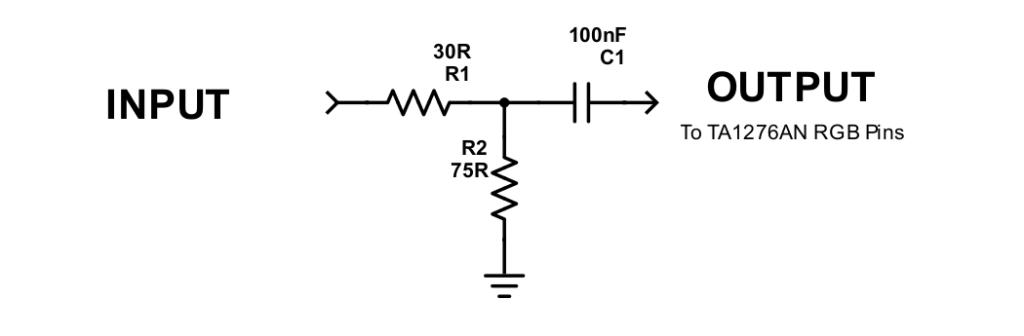
To add RGB, we need to connect to TA1276AN pin 35 (R), 34 (G), 33 (B). Capacitor C519, C518, C517 needs to be removed, and each color line should include the “standard” 0.1 uF in-line capacitor and a voltage divider, like this:
RGB input line attenuation and DC bias circuit.
Now the above picture is actually not the best circuit, as it attenuates the signals more than necessary, and the resulting termination resistance for the lines is 105 Ohm (30+75) instead of the correct value of 75 Ohm. The thing is that the TA1276AN takes 0.5Vpp signals instead of the normal 0.7Vpp, so the voltage divider accounts for this. Many suggest (including myself on earlier posts) using R1 = 24 Ohm and R2 = 51 Ohm, as that creates ~0.5Vpp from 0.7Vpp and 75 Ohm termination, however I’ve begun using R1 = 10 Ohm and R2 = 64.9 Ohm, as this gives ~0.6Vpp which is stated as the maximum input for TA1276AN (I’ve tried direct 0.7Vpp also which works fine, but better go by the specs). This results in a brighter picture, but I’d rather turn down brightness on the monitor, than not being able to turn it up. Your milage and wishes may vary.
Sync should be connected directly to the input pin on either input A or B (on the PCB side of the BNC plug). Which you select will then decide which input should be selected for RGB.
To be able to blank (switch to RGB) you need to lift pin 32 of the jungle, and add a pull-down resistor from this to GND. I usually use 10K here, but the schematics from Victor says 51K. Use whatever 10K+ resistor you got. Now on pin 32, when ~0.75V or higher is applied it switches to RGB. You can use a switch for this, or use pin 16 from SCART, whatever you fancy.
That’s basically it. Check the full schematics from Victor here:
So since I released the IF-C01COMG designs some years ago, several people asked me to make a full-sized card, I decided to finally do so. The result is this:
The IF-C01COMG THT clone
So this is basically my original THT base board thrown onto a full size PCB. The original was divided into two parts, mainly because of PCB pricing, which has now been reduced significantly by manufacturers like JLCPCB and so on. To use the available space, the complete BOM is written directly on the silkscreen along with various assembly instructions.
The board supports having either SCART or BNC connectors mounted, and has different audio options: When using SCART, the switch between the two RCAs select either passing the stereo from SCART to the RCAs or send it through a mono-mixing circuit to the internal speaker of the monitor, selected through SW1 switch. When using BNCs, the RCAs can be used as an input instead, running through the same mixing circuit. In that case SW1 should not be mounted, and needs bridging of a couple of pads (explained on the board).
I chose to use THT as I know some people find using SMD components a daunting task, so this should be possible to solder for most people.
You can find the complete Kicad project here, including the gerber files (found in the plot directory). The if-c01comg.zip fil can be directly uploaded to PCB manufacturers that don’t support direct kicad_pcb files (like JLCPCB).
So, latest addition to the family of BKM-129X compatibles, is a full size BNC version.
BKM-129X compatible, full size version
This is functionally quite close to the original, as it now has BNC outputs also. Since I couldn’t find BNC plugs featuring auto-termination (at a reasonable cost at least), I decided to add a switch to each signal which will either terminate to 75 Ohm, or enable passthrough of the signal to the OUT port.
Top view
It is then possible to set the switches to OFF (down) and use external terminators, or simply skip mounting the switches altogether, and add a jumper/0 Ohm resistor to the lower left two pins of each switch footprint, and then use external terminators.
The board requires the same Arduino with the BKM-129X-MCU code, directly programmed to the Arduino with a programmer (read some of my previous posts regarding this).
The MCU code is here: https://github.com/skumlos/bkm-129x-mcu
The Kicad project for the board here: https://github.com/skumlos/bkm-129x-simple-full
The 3D printable bracket here: https://www.thingiverse.com/thing:4462796
Card inserted to PVM-9L2Two 9L2s connected, bottom is the full size card (before bracket)SNES with passthrough
Please copy, share, produce and become rich, of this 🙂
So now after having most of the BKM-129X compatible monitors tested out properly, and some minor hardware adjustments fixed, I’ve made a spin-off of the BKM-129X compatible board, a direct SCART version with audio passthrough, and selectable mono mixing circuit.
The BKM-129X compatible SCART edition
Now there’s really not much difference to this board and the BNC version; the BNC plugs have been replaced with a SCART plug (I’ve used a Ninigi SCART, https://www.tme.eu/dk/en/details/scart-17/euro-hdmi-connectors/ninigi/) and then the two RCAs are added which feature the stereo audio passthrough from SCART. Along is a selectable mono mixing circuit, which is activated by the push button switch between the RCAs. The switch is supposed to be added between the RCAs. When pushed in, the stereo sound from the SCART is mixed to mono, when out, it is direct stereo. The mono mode is meant for monitors with audio inputs (which is always mono afaik) so a short RCA cable should be connected between the black connector and the monitor.
I’ve created a 3D printable bracket to fit in the slots for these cards, which will make everything sit flush with the monitor. The files can be found here: https://www.thingiverse.com/thing:4460188
So I wanted to see what kind of delay the built-in bootloader of the Nano v3.0 clones I have was causing, so I created a small sketch which basically sets up a pin as output and turns it on. I then attached my logic analyzer and measured the time from reset is released until the pin goes high.
Here is the measurement of the sketch, uploaded through the serial port, meaning through the bootloader, meaning bootloader is active:
Nano v3 clone with bootloader active
So here, from I release the reset, until the test pin goes high, is a delay of ~1,46 seconds.
And now, with the sketch uploaded through ISP/ICSP, meaning bootloader is now destroyed (and board cannot be programmed through serial port unless a new bootloader is added):
Nano v3 clone without bootloader
So now, from I release reset, until the test pin goes high, is a delay of 70 ms. Purrty big diffewence!
You can verify that the bootloader is now gone by checking the red LED on the board. When power is applied, it will blink once during startup (that’s the bootloader) and then do whatever your program does afterwards, so if it doesn’t, the bootloader is gone.
Now there are other bootloaders available, much faster ones also, but this is the one built into all clone Nanos I’ve worked with.
Turning the Arduino Nano clone into a programmer
So in case you don’t have a programmer (ISP) you can turn one of those Arduinos you have in the drawer into one! The Arduino IDE has a sketch that can be uploaded to any Arduino basically and make it act like a programmer, which you can then use to program sketches directly into other Arduinos, thus removing the bootloader, and reducing boot time dramatically. Here’s how to do it for a Nano:
Start the IDE, press “File“, press “Examples“, choose “11. ArduinoISP” and then “ArduinoISP“. It will then load that sketch. Press “Tools“, press “Board“, select “Arduino Nano“. Press “Tools“, press “Processor“, select “ATmega328P (Old bootloader)“. The “Old bootloader” versions have been the ones I needed to select for all clones I’ve used. You also need to select the serial port it is attached to in “Tools“. Press “Upload” to put the sketch in. You should now have an Arduino ISP. To get a stable connection, it is necessary to add a ~10uF capacitor between the RST and GND pins (negative on GND, positive on RST) on the Arduino ISP. Like this:
10uF cap between GND and RST on the ISP Nano
This is a hardware-hack to circumvent the Arduino from resetting when the serial data from the computer arrives. It is important that this is done after the ArduinoISP sketch has been uploaded.
Now to use your new programmer, open the sketch you want to write, select the correct board of your target (in this case no difference), and in “Tools“, press “Programmer“, select “Arduino as ISP” (note: NOT “ArduinoISP”, as that is a separate piece of hardware). The serial port should be the same as your Arduino programmer is connected to. You then need to connect the following with jumper cables (programmer -> target):
ISP Nano to the left and the target Nano to the right (and a Mini Pro top left, disregard that)
Then write the sketch by pressing “Sketch“, select“Upload using programmer“. It should upload the sketch to the target, which now has zero bootloader, thus boots close to immediately. To reclaim the bootloader (or change it to another), simply press the “Burn bootloader” in “Tools“.
TL;DR Gerber files here (NOTE: These gerbers are outdated, and using the Github project is recommended!)
So in continuation of my previous post about reverse engineering the Sony BKM-129X the next logical step would be to actually create a functional card that is compatible with monitors that use the BKM-129X card. The first step I took was making a “clone” of the input circuit of the original card, but there are a lot of components, and especially one of them I had trouble finding a suitable replacement for (the 2SA1462 transistor). I am still unsure if the extremely fast switching speed (1.8GHz!) is needed, so I finished the design, with the intention of trying to build it at some point. The Kicad project can be found on Github, here’s Kicads 3D render.
3D render from Kicad of the BKM-129X “clone”
Now the design is 100% untested, but I am sure I’ll get around to actually building one at some point, even just to verify the design. If anyone actually builds one, please let me know how it went.
Making it cheap
When I was reverse engineering the card I ended up having a close to complete “harness” wired into the monitor, except for the video signals. While designing the clone card above, I came up with the thought of simply wiring buffered signals straight into the inputs, as this is really the only thing the board does besides some on/off switching of the signals. So an obvious buffer system nowadays is the quite common THS7374 IC I had lying around anyways for other retro projects, so I hooked up the signals from that into the monitor, and it actually looked quite good. The only thing then missing would be the switches to disable all the outputs, and toggling external sync on and off. Since the THS7374 buffers all 4 channels, the obvious choice would be to insert a simple quad SPST analog switch IC after the THS7374, with three of the switches’ enable signals coupled together to the ~BX_OE signal from the MCU (for the RGB lines), and the last to ~EXT_SYNC_OE coupled to the sync line output. This would then make the whole card require only 2 IC’s (and a couple of capacitors and resistors) to form the complete video signal path circuit. The switch IC I ended up with is the ADG1611, which is a rather expensive chip (~$6) however it has a very low on resistance (1 Ohm) on each channel, and although I add current limiting resistors afterwards, when I designed it, I preferred having to add resistance than being unable to reduce it (had I chosen a switch IC with a higher on resistance). The switch can be powered up to +/- 8V, to be able to carry negative signals also, which is perfect as the BKM-129X is fed +/- 6V from the monitor. The THS7374 can run off 3-5V, so I put a cheap 3.3V LDO in, fed from the +6V so only a single regulator is needed. I ended up “cloning” most of the circuit between the monitor and the MCU, as some monitors allow multiple cards, and I wanted to be sure the load would match the original cards. It’s mostly some resistors and then the 74VHC125 chip which is cheap anyway. Thus the finished prototype card ended up looking like this:
The cheap BKM-129X compatible (prototype) Note the MIC3940-3.3 listing is wrong, it’s MIC3490-3.3, and 74LVC125 is a 75VHC125 in a TSSOP14 package
The connections (from top) are Y/G, B/B-Y, R/R-Y, sync.
I made a 3D printed bracket, which at the moment only fits my prototypes, as they’re a bit too deep (that is fixed in the Kicad project). I will redo it for the current one soon. The prototype when mounted in my PVM-9L2 then looks like this:
The card mounted in my PVM-9L2, only the prototype protrudes like this.
The bracket “grabs” the board and keeps it in place both from being pulled out when plugs are unmounted but also from moving side to side.
How the bracket holds the card
I have, for now, only tested on the PVM-9L2. The MCU code has been verified to work on a BVM-D14H5 also, so I am pretty sure it will work on the rest also. UPDATE Please read the part in the reverse engineering post regarding this (essentially you need to remove the bootloader).
Here are some photos from the card running in my PVM-9L2. Note they’re taken with my phone, and doesn’t represent how good it actually looks, but you’ll get the idea.
Streets of Rage 2 on SEGA Mega Drive 2 (60Hz modded)CloseupMega Man X on SNES Gee what game is that?Component/YPbPr with internal sync works fine also
You are welcome to copy, produce, sell the boards based on my work, actually please do!
Preliminary results with the BVM-D9H series is that it’s not sync’ing. To make it work, R9 should be removed and a jumper inserted (most likely smaller 10-33 Ohms will be good also). Doing this should not affect other monitors.
Remember to refer to the previous posts about how to program the Arduino for maximum compatibility.
If you have any experiences with the project you want to share, feel free to contact me on Facebook (Martin Hejnfelt), Discord (skum), shmups (skum), email to martin@hejnfelt.com or whereever you might find me. Please no more “Do the BKM-68X” though 😛
So I got a couple of PVM-9L2’s, both coming with the BKM-120D SDI card, but no analogue RGB inputs are present by default. They can be had by changing the BKM-120D with a BKM-129X card, which supplies standard RGBS/YPbPr in/out BNC sockets. The board is rather expensive, going in the $150’s range on eBay, although not that rare as such. The same board is used in other BVMs and some other PVMs can also use them, if not to add even more RGB inputs.
An original Sony BKM-129X RGB/YPbPr input card
Anyway, looked into if it was possible to make a clone of it, so I looked at the service manual, and could see that it was more complex than for instance the JVC card (IF-C01COMG) I cloned some time ago.
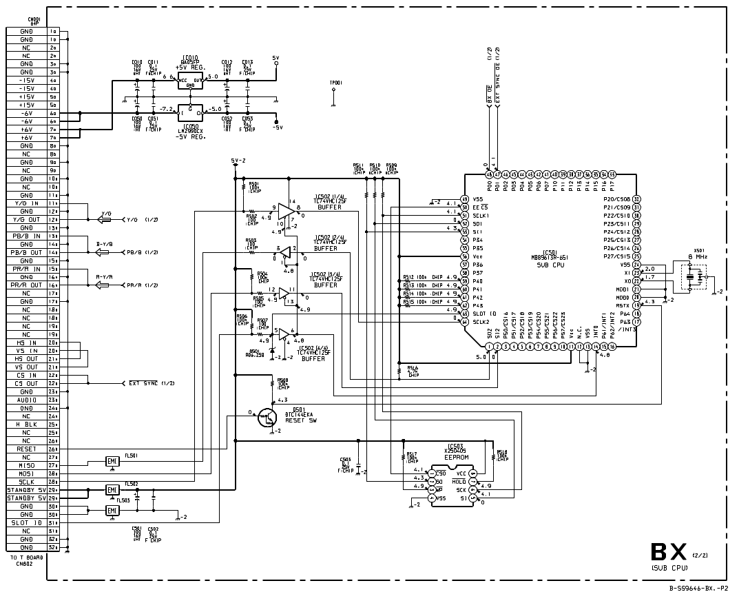
Here’s the MCU setup on the BKM-129X (from the service manual which can be downloaded on manualslib.com and most likely other places, it is shared with BKM-142HD, 120D and 127W).
It actually has a microcontroller/MCU on board, coupled to the monitor through the 64-pin socket, seemingly communicating on a SPI channel. SPI usually has 4 wires: a clock (SCLK), data master->slave (MOSI, master out, slave in), data slave->master (MISO, master in, slave out), and a slave-select (SS, meaning “selecting” the slave for communication, usually active low). So two data channels in each “direction” means SPI is “full duplex” which again means that data is flowing in both directions simultaneously (look up SPI on Wikipedia if you don’t know it). Slave-select is not present by default, but there is a SLOT ID pin going from the socket and into the MCU at two places, one called INT0, which is an interrupt pin, and another also called SLOT ID, so I guessed this to be functioning as slave select.
This data channel is then used by the monitor to verify the board is there and read some information from it and so on, thus activating RGB/YPbPr on said monitor, when the card is present (and selected). If the card supplies YPbPr or RGB is then setup in the monitor itself through the OSD, and there is also a serial number readout. At the same time, the microcontroller also has two “digital” outputs, one actually enabling the video output of the card (BX_OE, active low), and one (de)selecting external sync (EXT_SYNC_OE, active low).
To get anywhere I needed to get a card, so I bought one on eBay at too much money (the one shown in the beginning), which further fueled my desire to reverse engineer it, both for myself and the community.
The MCU of the board is some 8 MHz proprietary thing, and it has an EEPROM next to it, most likely with the program of the MCU on it, but since the MCU is not something easily bought, I didn’t try to read it out.
I expected the initialization sequence to be something like: 1. Monitor selects the card by setting SLOT ID to LOW. 2. Monitor reads some info including serial number. 3. Monitor decides card is there depending on response. 4. Monitor starts using card, sends commands commands to turn on and off the output and the external sync depending on button selection.
And then following commands for external sync and whatnot being something like: 1. Monitor selects the card by setting SLOT ID to LOW. 2. Monitor issues some “simple” command. 3. Monitor deselects card.
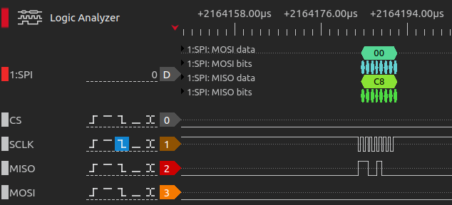
So to figure out the what commands look like, what response to give, and timings, I attached a logic analyzer to the RESET pin, MOSI, MISO, SCLK, SLOT ID, BX_OE and EXT_SYNC_OE pins. I have a DreamsourceLab DSLogic Plus USB logic analyzer, which can capture for a long period of time which is great, as I need to capture during the whole startup and initialization of the monitor to catch the information (which is around 5 seconds). At the same time, the software for it (DSView) also has built-in SPI decoding, so it can show me the byte representation of the data being transmitted over the wires. The connector is a DIN-41612 style a+b connector, where the bottom row is the a row, and the top is b. Pin numbers are counted from left to right. When the connector is vertical like it is positioned in the monitor, the leftmost column is then a row and rightmost is b, and pin numbers are counted from top to bottom.
So I set up the logic analyzer to capture for 5 seconds, and at 10 MHz (as SPI is often in the 1 MHz range this should be plenty oversampling). So doing this yielded a datastream like this CSV shows:
Now SPI actually has 4 possible modes, which will influence how data is interpreted: clock polarity (CPOL) and when to sample the data (CPHA), both can be 0 or 1, thus 4 possible configurations. So to figure out if the representation of the data is correct, these need to be setup properly. First of all, it can be seen that the SCLK is high when nothing is happening/idling, meaning CPOL should be 1. To decide if CPHA should be 0 or 1, you need to look at the transitions of SCLK and the data lines in relation to each other. I decided CPHA should be 1 based on the waveform, meaning data is sampled on the rising clock edge. I then did this multiple times, with different sample speeds also, to confirm I got the same readings again and again.
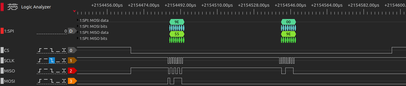
The output shows that SLOT ID seemingly *is* used as a slave select, the monitor then issues a 0x9E command, the slave responds with the same, while the master seems to clock in an address byte, which then is responded to from the card with whatever that address contains. This is a “classic” memory read pattern. There also seems to be a 0xBE request, which also throws out some data, so I expect that it’s another memory region that is requested or something like that. It then has some 0xF7, 0xF6 and 0xF4 requests, which seems to be depending on if it is selected, and if external sync is enabled or not.
My current idea of the protocol is then like this: 0x9E – Memory read (followed by an address to read). Example: 0x9E, 0x02, 0x00 reads memory address 0x02 (the last 0x00, is where the master clocks out the response), so response would be 0x9E, 0x39. 0xBE – Memory read of “another” region (followed by an address to read). The next here are preceded by 0x00, 0x00: 0xF7 – Deselect (turn off outputs). 0xF6 – Selected, output enable (BX_OE=LOW/0), external sync disabled (EXT_SYNC_OE=HIGH/1). 0xF5 – Also some deselect, see it rarely. 0xF4 – Selected, output enable (BX_OE=LOW/0), external sync enabled (EXT_SYNC_OE=LOW/0).
Upon startup, the card always gets two deselect (0xF7) and then a one of the select commands, depending on the external sync state.
So my first attempt was simply implementing all this in an Arduino Nano, putting the protocol into a request/response state machine, that each time the monitor asked for a specific byte, would return the same as the original BKM-129X did. This proved not to work. I got the request, 0x9E, and it was sent back, but then SLOT ID goes HIGH, and never LOW again to read the response. Hot damn…
So I looked some more at the waveforms, and noticed that the same happens for the original card, however SLOT ID goes LOW again some time after the 0x9E response, and then stays LOW for quite some time, until SCLK suddenly starts clocking in the response data. Since this was not happening on my setup, I thought that maybe this was some part of a handshake, because of the SLOT ID labeled pin on the MCU itself. So my guess was that the MCU should slave-select itself when the actual response was required, sounds somewhat strange, but hey, it’s Sony. And whaddayaknow, it worked!
A single byte read. The first CS low is the monitor sinking SLOT ID, the second is the card.Here’s a closeup of the initial part (representing the first CS low in the previous picture).And here the second part, where CS is driven low by the cards SLOT ID pin. Look at the time in the top, around 10 ms has passed since the command was issued.
Doing this, I could now, having only the Arduino Nano connected, select RGB (no picture of course), read out a serial (that was identical to my original card) and select and deselect external sync. So to do it, SLOT ID pin is first configured as input, and when the actual response is needed, it waits for the SLOT ID from the monitor to go HIGH, then the pin is configured as an output, output is set LOW (thus slave selecting itself), waits for the response to be read out over SPI, and then it sets SLOT ID as HIGH, and back to an input.
Now I have no idea what most of the data reads represent, except it seems (at least) the first byte read, address 0x00, returns 0xC8 for the BKM-129X and 0xC0 for the BKM-120D, so I expect this is what the monitor uses to identify the card. The next addresses read, 0x02-0x09, represents the serial number, written in ASCII bytes (so 0x30 for 0, 0x31 for 1, 0x32 for 2 and so on, www.asciitable.com). Looking at the CSV from earlier, it can be seen that my original card has the serial number 2001911 (0x32, 0x30, 0x30, 0x31, 0x39, 0x31, 0x31).
The PVM-9L2 with just the Arduino attached.I changed the serial number to 5001337, and it reads fine.The Arduino connected in the back, including the 100 Ohm and the 100K resistor for at the SLOT ID pin and including a BC550 to allow the monitor to reset the MCU.
So since the code now has been refactored and changed a bit, and tested on more monitors, at least newer monitors like the BVM-D9H and D14H seem to require that the bootloader is removed and the application is running as the only piece of software (seemingly to boot faster). This can be accomplished by programming the software directly to the Arduino, without using the USB. This means a “real” programmer (ISP) is needed, and the ICSP header (or the corresponding pins) are used for programming. A cheap ISP can be made with another Arduino Nano, check out how to do that here: https://immerhax.com/?p=480 (scroll down a bit)
Any feedback is appreciated, please email to martin@hejnfelt.com or reach me on shmups (username: skum), on the CRT discord (username: skum) or on Facebook (Martin Hejnfelt).
Next up is designing the rest of the board to have a true compatible card. I am in the last stages of this, and will release here and github when done.
By default, the European Mega Drive (2) has a vertical refresh rate of 50 Hz, meaning the games play slower than its Japanese and American counterparts which play in 60 Hz. We don’t like that, so that needs to be fixed! So getting a Mega Drive 2 to play games in the original 60 Hz speed plus being able to switch the language on games that support it is somewhat easy, but there are some caveats, especially if you’re a purist. This guide relates to a PAL Mega Drive 2 with a VA1 board. Note that I’m still a sucker for hardwired switches, but a lot of this can also be done with a MegaDrive++ setup.
Getting 60 Hz out of the MD2
First of all, what vertical frequency the Mega Drive generates is depending on the voltage on pin 46 of the main CPU. When pin 46 is tied to 0 V/GND, it generates 50 Hz, while when it is logic high/5 V, it generates 60 Hz. On this board pin 46 is tied to GND not far from the main chip. This small bridge as can be seen below, needs to be cut.
Where to cut when isolating pin 46The connection to the GND plane is now cut
When the trace is cut like this, we isolate the pin. It is supposed to have a pull-up and if you measure between 5 V and the pin, you’ll be able to measure around 25 kOhm, so indeed it seems there is something here. At the same time, the trace is also connected to the MB3514 video encoder, which generates composite video and amplifies RGB. It is connected to pin 7 which (lucky for us) is also the pin that selects if the MB3514 should produce NTSC or PAL composite signal (and chroma in S-Video), 0 V for PAL, 5 V for NTSC. We’ll get back to this later.
Close to the power regulator (the heat sink thing) are 4 holes, which denotes two jumper points, JP3 and JP4. The left side is connected to the above trace, meaning to pin 46 and MB3514 pin 7. The right side is connected to GND for JP3 and 5V for JP4. Since the holes are through holes (most likely filled with solder) these are some good points to connect to. Now connecting 5 V to the left side will make the MD2 create 60 Hz video, and MB3514 create NTSC, while connecting 0 V will give 50 Hz video encoded to PAL. So connecting a switch here that selects between the two by connecting 0 V or 5 V from the right side makes it easy to switch between the two modes.
The jumper pads that makes connection easier
Now if we try to connect 5 V to one of the pads om the left side, we will see that the video is now full screen and running noticeably faster. However, if we are using composite, we might be getting a black and white image!
Dafuqs up with my black and white picture?
Usually people will attribute this to being because the TV or monitor the machine is connected to, cannot decode NTSC, and then switch to RGB. The decision is good (composite sucks), but for the wrong reasons (especially if we know the set to be NTSC compatible). So why are we seeing black and white composite video? The MB3514 is properly set to generate NTSC, however the chip also has a carrier frequency input (pin 6) which need to match the specifications the receiver expects.
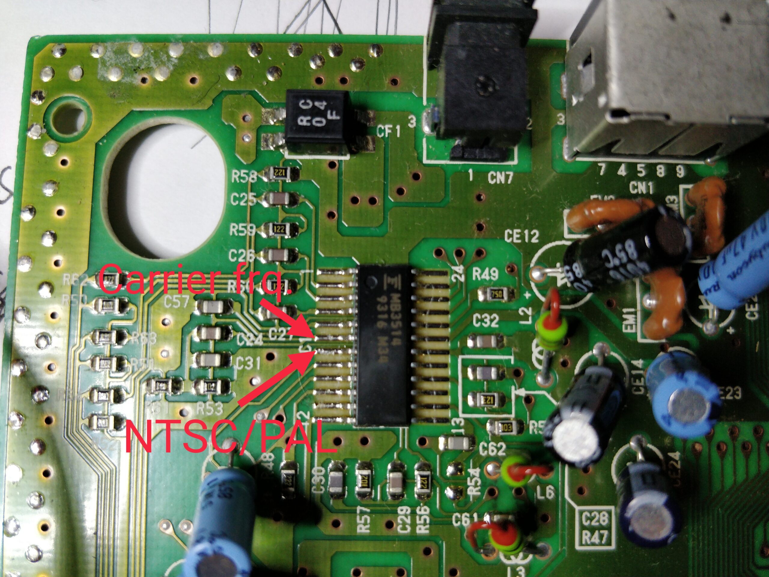
The MB3514 and the two pins for NTSC/PAL and carrier frequency
For PAL this frequency is ~4.43 MHz and for NTSC it is ~3.58 MHz. Since these subcarrier frequencies are used to encode only the colors of the video signal, and we are getting black and white, something is off. If we try to measure the frequency going to pin 6 we see this when in PAL mode:
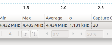
MB3514 carrier frequency in PAL mode
The average frequency, 4.434 MHz
Note the Measurement in the bottom where it says “Average” and “4.434 MHz”, so here the carrier frequency is correct.
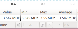
If we switch to 60 Hz / NTSC mode, we get this:
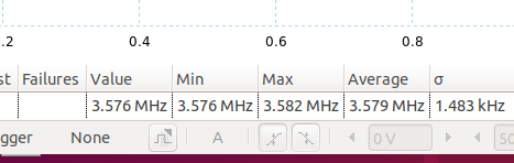
MB3514 carrier frequency in NTSC mode on PAL console
So we can see we have a carrier frequency of average 3.547 MHz, which is somewhat off the intended ~3.58 MHz, so this is why we are seeing a B/W picture; the receiver cannot lock onto the carrier frequency to decode color.
We can then deduce that the carrier frequency is created wrong, and since the frequency is created by the main CPU, the answer to why, can be found in the differences of the main oscillator which supplies the clock signal for the system. On PAL consoles this is ~53.20 MHz (which is equal to roughly 12 x 4.43 MHz), while on US and Jap consoles it’s ~53.69 MHz (which is equal to 15 x 3.58 MHz). Now what happens is, that when pin 46 is low (for 50 Hz PAL), it divides the clock by 12, and when driven high (for 60 Hz NTSC), it divides by 15 (53.20 MHz / 15 is roughly 3.55 MHz, which matches what we saw above). Now how to fix this?
Bring in the Dual Frequency Oscillator (DFO)
The Dual Frequency Oscillator is a small device based on Texas Instruments CDCE family of clock generators. It can be programmed to generate different clock signals depending on an input. A guy called micro has made a design that is a drop in replacement of the main oscillator (https://oshpark.com/profiles/micro) so building one of these, replace the original oscillator on the board, take the same signal as we send to pin 46, and insert at the DFO, we can now switch the main oscillator frequency to match the selected mode!
So we need to desolder the main oscillator and dump the DFO in. We can then take the signal to the DFO from the other unused through hole at either JP3 or JP4 and route that to S0.
The DFO installed
Doing this, we can then measure that the subcarrier frequency is now correct when in 60 Hz mode:
The white wire goes to S0 of DFO, the green to the switch, red/black to switch poles.
Fixed MB3514 carrier frequency
At the same time, this also fixes that the output frequency in fact was not 60 Hz, but more 59,2 MHz, which can help when connecting to some flatscreen TVs an converters like Framemeister. Note that much of this actually relates to many other 50 Hz PAL to 60 Hz NTSC conversions on Master System, PlayStation and so on.
So what about that Japanese language?
Pin 107 of the main chip selects if the machine should report as being an English machine or a Japanese machine. This “helps” some dual language games to show either Japanese or English text. An example is Quackshot. When pin 107 is connected to logic high (5 V), the machine reports English, when 0 V it reports Japanese. On this board, pin 107 is connected to 5 V through a via to a 5 V plane. This somewhat sucks, as we then either have to lift the pin, cut the trace, or cut around the via in the plane. I selected the second option: Cut the trace at the via and then scratch some of the solder mask off to be able to solder to the trace.
The trace to pin 107 is cut
The yellow wire soldered to the trace to pin 107
Bringing it all together
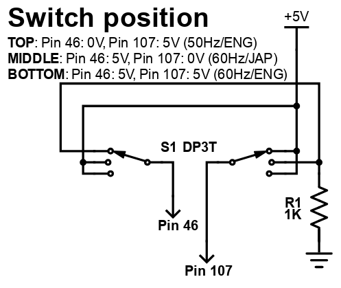
Now we have two places to insert information, the 50 / 60 Hz and the language. Some use two switches for this, one for each, however we can deduce that only 3 sane options exist:
50 Hz / English / Pin 46: 0 V, Pin 107: 5 V 60 Hz / Japanese / Pin 46: 5 V, Pin 107: 0 V 60 Hz / English / Pin 46: 5 V, Pin 107: 5 V
This can be done by a simple DP3T switch, so instead of having two switches, which techically gives the 4th “invalid” option of 50 Hz / Japanese, we hook up to one with 3 positions. The hookups look like this:
R1 is to prevent shorting the supply when switching while machine is on. It can be 1K-10K but it needs to be less than the internal pull-ups (which seems to be in the 25K range as mentioned earlier).
The DP3T, still missing language wire here
So I like to conceal the switch as much as possible which I do by using the left side facing the switch downwards.
The installed switch
Of course some mechanical holes needs to be drilled and filed in. How big this is depends on your switch.
The holes for the switchThe switch seen from the bottom
So now, by switching we can select all three regions with correct corresponding frequencies. All good!
Update: I’ve been told that this also works for TM-2100PN.
I got a hold of a JVC TM-1700PN, which is a 550TVL composite/S-Video monitor. As always this baby needs RGB modding! So let’s get to it.
It uses a TDA8366 as the jungle IC, which has direct linear RGB input. OSD is mixed in after the jungle, so there is no need for muxing. The monitor exists in an already RGB capable version, the TM-1750PN, and actually most of the circuit is already there, but not populated. Anyways, looking at the service manual, the RGB inputs are pin 21-23 and blanking at pin 24. The pins are connected to three capacitors, C131-C133, however in the TM-1700PN they are not capacitors but simple jumpers that end up at some 22K resistors to GND. So we remove these jumpers, and this is where we inject our RGB. C131 is the blue line, C133 is the red, and C132 is the green.
RGB lines
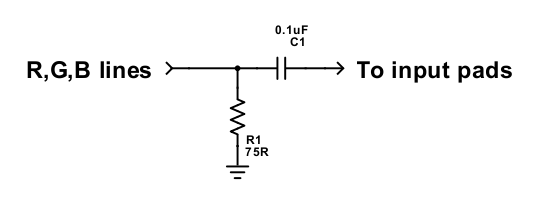
Note that the RGB should be normal 0.7Vpp but 75 Ohm terminated, and with a 0.1uF capacitor before injection. I have this circuit on the SCART breakout that I use (check some of my other posts), but in general the input circuit for each line looks like this:
Input circuit for RGB lines
Sync should be added directly (no circuit) to one of the inputs, I chose directly at Input A on the PCB side of the BNC plug.
Sync input
Now the next thing is getting it to blank RGB input. The TDA8633 has blanking on pin 24, however this is tied to the already present circuit of the MCU, as the pin is also used to blank the RGB output of the jungle, because OSD is added after it. This is a bit different than the other JVCs I’ve worked on, so off to the datasheet. It seems that the RGB blanking happens when pin 24 is between 0.9V and 3V. Above 4V is OSD blanking, so we need to stay within the 0.9V-3V. The monitor does this in itself by having a voltage divider between a 1.2K Ohm resistor (R725) to GND and a 1.8K Ohm resistor (R726) connected to a switch to 5V. This gives a signal around 2V, which will blank it. So to force this, we could inject 5V at that 1.8K resistor, but that is placed on the mainboard, so requires more disassembly of the monitor. Instead there is an unpopulated resistor R130 connected to the “top” of the 1.2K Ohm, so we can create a “new” voltage divider here, by added a 1.8K (I used a 2K) and inject the blanking signal through that. I at the same time added a Schottky diode as this point is where the MCU then also connects 5V for OSD blanking, and I wanted to avoid backfeeding voltage to my console. You can use more or less any diode, I choose Schottky for the low voltage drop, and of course the higher the voltage drop over the diode, the lower voltage ends up at the jungle, increasing the risk of hitting the low threshold for blanking. The circuit equivalent is something like this:
The circuit for blanking. We add D1 and R1. R2 represents R725 in the monitor.
And here’s real life:
Blanking circuit, 2K resistor and a Schottky diode, heat shrink or something should be added.
So when around 3-5V is added at the diode, it will blank to RGB. Hooray!
So all this is connected to the SCART breakout I’ve mentioned earlier, and presto, a fine RGB picture 🙂
All the connections as of yet
The black wire is GND from the SCART board, and just goes to whatever GND point on the board.
Audio using the SCART board, audio is mixed to mono and injected at the RCA pin for input A.
Audio injection point
So everything is connected to the SCART breakout board I’ve designed (OSHPark) and a case that fits the grille. This monitor has a slightly different pitch of the holes, so I had to modify the case a bit. Will put the 3D model it along with the original one (70mm between holes) on Thingiverse (it’s gonna be postfixed with 72mm).
The SCART connector with audio passthrough
So here are the finished connections:
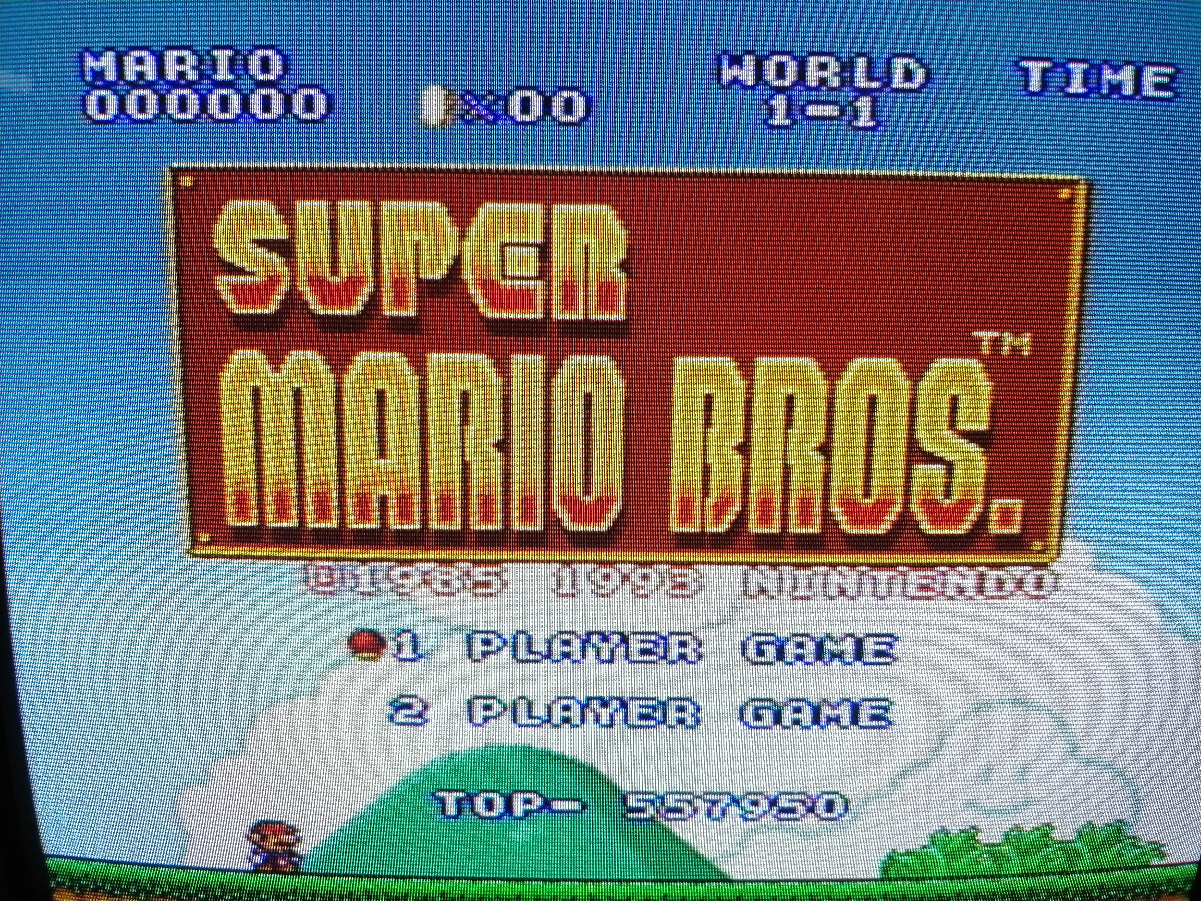
The finished wiring incl. some hot-glue strain reliefSuper Mario All-starsHere ist roughly the same picture in composite. Notice the dotcrawl…Super Mario 3Turtles in TimeMore tortoise actionMore original composite, more dotcrawl.
When applying the preempt_rt patch to the Linux kernel, EFI variables at runtime are disabled by default, seemingly due to high latencies (https://www.spinics.net/lists/linux-rt-users/msg19980.html). If you still need EFI variables accessible for userspace applications like efibootmgr, add “efi=runtime” to the kernel parameters/arguments. This will re-enable the possibility to mount efivarfs with “mount -t efivarfs none /sys/firmware/efi/efivars”. This will of course not magically make the above mentioned latencies disappear, so use this at your own discretion.